Introduction to 89C51 Microcontroller:
The ATMEL 89C51 is used here; some of the features with respect to our project are discussed here.
3.1 Memory Organization
The ATMEL 89C51 implements a separate memory space for code and data, both code and data may be internal; however, both expand using external components to a maximum of 64k code memory and 64k data memory. The memory consists of on-chip ROM (4KB) and on-chip RAM (128B). The on-chip RAM contains rich arrangements of general-purpose storage, bit addressable storage, register banks, and special function registers (SFR’s). The notable features are
• The registers and input/output ports are memory mapped
• The stack memory resides within the internal RAM
3.1.1 General-Purpose RAM
There are total of 80 bytes of general-purpose RAM from address 30H to 7FH. Any location in this part can be addressed using direct or indirect addressing modes.
3.1.2 Bit-Addressable RAM
The ATMEL 89C51 contain 210 bit-addressable locations, of which 128 are at byte addresses 20H through 2F, and the rest are in SFR’s. Bits can be set, cleared, ANDed, ORed, etc with a single instruction. These bits can be accessed as bytes or as bits.
3.1.3 Register Banks
The bottom 32 locations of internal memory contain the register banks, each having registers from R0 to R7. The different banks are selected using register bank select bits (RS0 and RS1) in program status word.
3.1.4 Special Function Registers
The ATMEL 89C51 internal registers are configured as a part of on chip RAM: therefore each register also has an address. There are 21 special function registers, each having a name and direct address, for example accumulator has name A and address ACC.
3.2 Input/output Ports
3.2.1 Port 0
Port 0 is a dual-purpose serving as general-purpose I/O port. For larger design it is used to multiplex the low byte of 16-bit address.
3.2.2 Port 1
Port 1 is a dedicated I/O port, used for interfacing to external devices. No alternate functionality is defined for the port.
3.2.3 Port 2
Port 2 is a dual-purpose port serving as general –purpose I/O port, or as high byte of address bus for designs with external code memory exceeding 256 bytes.
3.2.4 Port 3
Port 3 is a dual-purpose port serving also as general-purpose I/O port, the individual pins of the port 3 also has some special features.
3.3 Interrupts
There are total of five interrupts in ATMEL 89C51 as given below
• Two for external interrupts INT0 and INT1
• Two for timer1 and timer0
• One for serial port
3.4 Two 16-bit Timers
The ATMEL 89C51 have two 16-bit timers, controlled by TCON register. They can be operated in four different modes named: 13-bit timer mode, 16-bit timer mode, 8-bit auto-reload mode, and split-timer mode. The mode and clocking sources of timer0 and timer1 are set by TMOD register. Other registers that are used in timer operation are THx, and TLx. The timer is started by setting the flag TRx and when an overflow occurs the TFx flag is set automatically.
3.5 Serial Interface
The ATMEL 89C51 serial port has four modes of operation, named 8-bit shift register mode (fixed baud rate), 8-bit UART mode (variable baud rate), 9-bit UART mode (fixed baud rate), and 9-bit UART mode (variable baud rate). The timer1 is used for setting the variable baud rate. The different flags used in serial interfacing are TI and RI.
3.5.1 MAX 232 Serial Interface IC
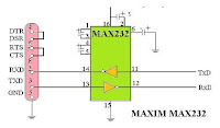
MAX 232 converts serial data into parallel in receiving mode while it converts parallel data into serial in transmitting mode. Standard serial interfacing for PC, MAX232, requires negative logic, i.e., logic '1' is -5V to -12V and logic '0' is +5V to +12V. To convert TTL logic, say, TxD and RxD pins of the microcontroller chips thus need a converter chip. A MAX232 chip has long been using in many microcontroller boards. It provides 2-channel RS232C port and requires external 10uF capacitors. Carefully check the polarity of capacitor when soldering the board.
Tags:-MAX232 Serial level converter ,Serial Programming/MAX232 Driver Receiver ,Interfacing The Serial / RS-232 Port,pin diagram of atmel 89C51 atmel 89C51 pin diagram 8051 Tutorial: Interrupts 8051 Microcontroller Architecture The 8051 Microcontroller and Embedded Systems INTERRUPTS PROGRAMMING IN ASSEMBLY Define the interrupt priority of the 8051 MEMORY AND REGISTER ORGANISATION 8051 Memory Organisation. Internal ROM. The 8051 has 4K (4096 locations) of on-chip ROM. This is used for storing the system program. 8051 MEMORY ORGANIZATION, PROGRAM MEMORY, DATA MEMORY 8051 Memory Write Example Program


No comments:
Post a Comment