Tuesday, January 24, 2012

Control System of Numeration


The Romans devised a system that was a substantial improvement over hash marks, because it used a variety of symbols (or ciphers) to represent increasingly large quantities. The notation for 1 is the capital letter I. The notation for 5 is the capital letter V. Other ciphers possess increasing values:

X = 10
L = 50
C = 100
D = 500
M = 1000

If a cipher is accompanied by another cipher of equal or lesser value to the immediate right of it, with no ciphers greater than that other cipher to the right of that other cipher, that other cipher's value is added to the total quantity. Thus, VIII symbolizes the number 8, and CLVII symbolizes the number 157. On the other hand, if a cipher is accompanied by another cipher of lesser value to the immediate left, that other cipher's value is subtracted from the first. Therefore, IV symbolizes the number 4 (V minus I), and CM symbolizes the number 900 (M minus C). You might have noticed that ending credit sequences for most motion pictures contain a notice for the date of production, in Roman numerals. For the year 1987, it would read: MCMLXXXVII. Let's break this numeral down into its constituent parts, from left to right:

M = 1000
+
CM = 900
+
L = 50
+
XXX = 30
+
V = 5
+
II = 2

Aren't you glad we don't use this system of numeration? Large numbers are very difficult to denote this way, and the left vs. right / subtraction vs. addition of values can be very confusing, too. Another major problem with this system is that there is no provision for representing the number zero or negative numbers, both very important concepts in mathematics. Roman culture, however, was more pragmatic with respect to mathematics than most, choosing only to develop their numeration system as far as it was necessary for use in daily life. 
 
We owe one of the most important ideas in numeration to the ancient Babylonians, who were the first (as far as we know) to develop the concept of cipher position, or place value, in representing larger numbers. Instead of inventing new ciphers to represent larger numbers, as the Romans did, they re-used the same ciphers, placing them in different positions from right to left. Our own decimal numeration system uses this concept, with only ten ciphers (0, 1, 2, 3, 4, 5, 6, 7, 8, and 9) used in "weighted" positions to represent very large and very small numbers. Each cipher represents an integer quantity, and each place from right to left in the notation represents a multiplying constant, or weight, for each integer quantity. For example, if we see the decimal notation "1206", we known that this may be broken down into its constituent weight-products as such:

1206 = 1000 + 200 + 6
1206  =  (1 x 1000) + (2 x 100) + (0 x 10) + (6 x 1)

Each cipher is called a digit in the decimal numeration system, and each weight, or place value, is ten times that of the one to the immediate right. So, we have a ones place, a tens place, a hundreds place, a thousands place, and so on, working from right to left. Right about now, you're probably wondering why I'm laboring to describe the obvious. Who needs to be told how decimal numeration works, after you've studied math as advanced as algebra and trigonometry? The reason is to better understand other numeration systems, by first knowing the how's and why's of the one you're already used to. 
 
The decimal numeration system uses ten ciphers, and place-weights that are multiples of ten. What if we made a numeration system with the same strategy of weighted places, except with fewer or more ciphers? The binary numeration system is such a system. Instead of ten different cipher symbols, with each weight constant being ten times the one before it, we only have two cipher symbols, and each weight constant is twice as much as the one before it. The two allowable cipher symbols for the binary system of numeration are "1" and "0," and these ciphers are arranged right-to-left in doubling values of weight. The rightmost place is the ones place, just as with decimal notation.


read more "Control System of Numeration"

Monday, January 23, 2012

Schematic Liquid Crystal Display LCD Introduction

3 LCD Overview
The HD44780 dot-matrix liquid crystal display controller and driver LSI displays alphanumeric characters and symbols. It can be configured to drive a dot-matrix liquid crystal display when interfaced with a processor. A single HD44780 can display up to one 20-character line or two 20-character lines.
3.1 Function Description
The following section introduces some of the important features of the liquid crystal display that are important for interfacing with the liquid crystal display through software.
3.1.1 Registers
The LCD has two 8-bit registers, an instruction register (IR) and a data register (DR).The IR stores instruction information, such as display clear and cursor shift, and address information for display data RAM (DDRAM) and character generator RAM (CGRAM). The DR temporarily stores data to be entered into DDRAM or CGRAM and temporarily stores data to be read from DDRAM or CGRAM. Data written into the DR is automatically written into DDRAM or CGRAM by an internal operation. The DR is also used for data storage when reading data from DDRAM or CGRAM. When address information is written into the IR, data is read and then stored into the DR from DDRAM or CGRAM by an internal operation.
3.1.2 Busy Flag (BF)
When the busy flag is 1, the LCD is in the internal operation mode, and the next instruction will not be accepted. When RS = 0 and R/W = 1 (Table 1), the busy flag is output to DB7. The next instruction must be written after ensuring that the busy flag is 0.
3.1.3 Address Counter (AC)
The address counter (AC) assigns addresses to both DDRAM and CGRAM. When an address of an instruction is written into the IR, the address information is sent from the IR to the AC. Selection of either DDRAM or CGRAM is also determined concurrently by the instruction.
After writing into (reading from) DDRAM or CGRAM, the AC is automatically incremented by 1 (decremented by 1). The AC contents are then output to DB0 to DB6 when RS = 0 and R/W = 1.
3.1.4 Initializing by Internal Reset Circuit
An internal reset circuit automatically initializes the LCD when the power is turned on. The busy flag (BF) is kept in the busy state until the initialization ends (BF = 1). The busy state lasts for 10 ms after VCC rises to 4.5 V
3.2 Pin assignment
The pin assignment, shown in Table1, is the industry standard for character LCD-modules with a maximum of 80 characters.


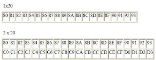
3.3 LCD addressing values
Liquid Crystal Display LCD Introduction PIN assignment of LCD

HD44780 lcd microcontroller interfacing instruction set

LCD addressing of characters location

Tags:-lcd display microcontroller program,liquid crystal display interfacing with microcontroller, how to use lcd with microcontroller,microcontroller at89c2051 based alarm clock: assembly code,microcontroller at89c2051 based ir wireless frequency counter: assembly code,
read more "Schematic Liquid Crystal Display LCD Introduction"

Saturday, January 21, 2012

Control Timer Circuit Using Real Time Clock PCF8583


This is a circuit for timer that is control by real time clock PCF8583. The PCF8583 is a clock/calendar circuit based on a 2048-bit static CMOS RAM organized as 256 words by 8 bits. Addresses and data are transferred serially via the two-line bidirectional I2C-bus. This is the figure of the circuit.


The built-in word address register is incremented automatically after each written or read data byte. Address pin A0 is used for programming the hardware address, allowing the connection of two devices to the bus without additional hardware. The built-in 32.768 kHz oscillator circuit and the first 8 bytes of the RAM are used for the clock/calendar and counter functions. The next 8 bytes may be programmed as alarm registers or used as free RAM space. The remaining 240 bytes are free RAM locations. The PCF8583 device is connected to a port of the AVR microcontroller.
read more "Control Timer Circuit Using Real Time Clock PCF8583"

Tuesday, January 17, 2012

Control Running LED Circuit


This running LED or LED chaser is a good project for beginners in the microcontroller technology. It is easy to build, and the assembler program code can be easily adapted. This running LED light has 15 red 3mm LED's. The 15 outputs of ports B and D are used to drive the LED. This is the figure of the circuit.


The LED's light up in a pattern that can be made in the program code, the LEDs run back and forth. With a push button you can select another pattern at which the LEDs runs. There are three running LED patterns which you can run: with one LED, three LED and five LED. The project uses the ATTiny2313 microcontroller but the ATTiny2313 can also be used. The AVR port can draw 20mA current so you only have to place a resistor at the port of the AVR to limit the current to 20mA. The LEDs are connected to ground so when the output of the port is high the LED will go on. The circuit uses a ceramic resonator of 10 MHz as oscillator. When you use ATTiny2313 you can discard the resonator because they have an on chip clock source. The fuse bits can be programmed to run the chip at 8Mhz.The circuit has to be powered with 5V DC regulated.


read more "Control Running LED Circuit"

Control LCD Display Circuit on The Glass Interface


Liquid Crystal Display on Glass is the newest in LCD technology. The display is very compact, it measures 55x27 mm and the height is only 2mm without LED backlight and 5.8mm with LED backlight. The display's can have different LED background light instead of only the green and blue of the normal LCD modules. 

There are 5 monochrome colors available: white, green/yellow, blue, red, amber and there is even a full color RGB background possible. The contrast of the display can be set with a command. This is done using software. The display's series consists of 3 types. This is the figure of the circuit.


The display and the corresponding backlight are clipped together and inserted into a PCB and soldered. The display has a build-in character set of 248 europe and japannese characters, in addition you can also define 8 characters. The integrated controller, the ST7036, has build in commands to control the display. In this project the display is connected to an AVR AT2313 microcontroller. 

For the ease of use it has designed a small PCB. The board has two rows of 20-pins socket connectors, in which the display can be inserted, it has also a resistor to limit the current through the background LEDs. For connection with the microcontroller the board has a 5x2-pin connector, so the board can easily connected to the STK500 board or to the AT2313 project board with a 10-pole flat cable. In this project the 4-mode is used so there are only 4 data lines and 2 control lines.


read more "Control LCD Display Circuit on The Glass Interface"

Control Fading Circuit for RGB LED


An RGB LED is a LED which has three LED's integrated in one packaging. These LED's has the colors red, green, and blue. Such a LED costs about 1 Euro. With these three colors you can mix to any color. When using 8-bit PWM a number of 256 * 256 * 256 combinations can be made, thus the LED can show 16.777 million colors, and 256 different brightness. When all the three LED is at full brightness the color will be white. When they are all off the color will be 'black' in the dark.

The RGB LED used here has four leads, one for each color an one for the common cathode (ground). The Red LED operates on a voltage of 2 V, Green needs 3.5 V, and the Blue LED needs also 3.5 V. Each LED draws 20mA current, so the maximum current consumption is 60mA. This is the figure of the circuit.


The circuit is very simple. The RGB LED is hooked up to the PWM outputs on PORTB1, PORTB2 and PORTB3 of the ATMega8. There is also a resistor between the LED and the ATM8 to limit the current to 20mA. There is also a link to the datasheet of the RGB LED that is used in this project.
read more "Control Fading Circuit for RGB LED"

Control Digital Thermometer Using LM35


The LM35 of National Semiconductors that is used in this project is a precision centigrade temperature sensor, which has an analog output voltage. It has a range of -55ºC to +150ºC and a accuracy of ±0.5ºC . The output voltage is 10mV/ºC . The output voltage is converted by the AD convertor of the AT Mega8. The temperature is displayed on an LCD module. In this example the thermometer has a range of 0ºC to 40ºC and a resolution of 0.5ºC. If you want to have a read out in Fahrenheit you can use the LM34.

This is a design for digital thermometer that can display using LCD. This is the figure of the circuit.


In the circuit the LM35 is connected to the ADC port of the ATMega8. The ATMega8 uses a crystal as an oscillator for the clock pulses. At PORTD of the ATM8 an 20x4 LCD display is hooked to display the temperature in a discrete value and in a analog bar.
read more "Control Digital Thermometer Using LM35"

Sunday, January 8, 2012

Schematic ALU of 8052 Microcontroller

2.2 ALU of 8052 Microcontroller
The ALU performs math functions, comparisons, and decision making. Two SFRs, the accumulator (ACC) and the B register, are the source and destination for most operations. The ALU provides information to the Program Status Word (PSW), which contains a carry bit, an auxiliary carry bit, a parity bit, an overflow bit, register selection bits, and two general use bits.
2.3 Accumulator of 8052 Microcontroller
The accumulator is the primary SFR. It is the source or destination address for most instructions. Arithmetic, Boolean, and branching instructions use the accumulator.
2.4 Program Status Word (PSW) of 8052 Microcontroller
The Program Status Word contains status bits, user flags, and a 2-bit value for register bank select. The status flags are Carry, Auxiliary Carry, Overflow, and Parity.
2.5 Stack Pointer (SP) of 8052 Microcontroller
The 8052 uses internal RAM for its stack. The stack location is not fixed and you may assign any convenient value to SP. The SP defaults to 7 on power up. The stack grows upward. The SP always points to the last location on the stack. PUSH increments the pointer and POP decrements it.
2.6 Data Pointer (DPTR) of 8052 Microcontroller
The Data Pointer designates a 16-bit address in Code or Data memory. The instruction designates the memory type and implements the selection by strobing.
2.7 Timer/Counters of 8052 Microcontroller
The 8052 has three 16-bit Timer/Counters, which may be configured as 8-bit, 13-bit, or 16-bit timers. Timer 2 has capture capability. Other SFRs control the timers, as detailed in the SFR page.
2.8 UART of 8052 Microcontroller
The UART is full duplex. It has a control register and both an input and output buffer, each accessed as SBUF. The correct buffer is determined by the context of the instruction. The serial port may be polled or serviced by an interrupt.
2.9 I/O Ports of 8052 Microcontroller
The 8052 has four I/O ports. When external memory is used, Port 0 and Port 2 serve as multiplexed address/data ports and may not be used for general purpose I/O. The ports have latches which retain the value written by software.
2.10 Program Counter (Pc) of 8052 Microcontroller
A 16-bit PC designates the address of the next instruction to be fetched. The PC is not directly accessible by the user but may be retrieved from the stack after a branching instruction or call. At power up the PC is 0000H. The PC increments with each instruction.
2.11 Scratchpad Registers (Ram) of 8052 Microcontroller
The 8052 contains 256 bytes of RAM in addition to the 128 bytes reserved for SFRs. Direct or indirect addressing accesses the lower 128 bytes. Only indirect addressing accesses the upper 128 bytes. The Stack, Working Register Banks, and Bit-addressable Registers are in the Scratchpad Registers.
2.12 Register Banks of 8052 Microcontroller
The first 32 bytes of Scratchpad RAM are four banks of 8 bytes each, numbered from 0 to 3. Two bits in the PSW register select the active bank. This permits rapid switching of software context. BASIC-52 uses banks 0...2 and never uses bank 3, which is reserved for the user.
2.13 Address/Data Bus of 8052 Microcontroller
The 8052 uses two signals to enable external memory: and. Both signals are active low. goes low with MOVC instructions. goes low with MOVX instructions. enables external code memory and enables external data memory. In both cases, Ports 0 and 2 provide a multiplexed address and data bus. Port 2 has the high byte of the 16-bit address and Port 0 the low. Data transfers occur on Port 0.
2.14 Internal Ram Organization of 8052 Microcontroller
The 8052 has 256 bytes of Scratchpad RAM and 128 bytes of SFR RAM,The SFR registers occupy 80H to 0FFH, the same range as the upper 128 bytes of Scratchpad RAM. The 8052 does not use all of the SFR RAM. Unused SFR registers are reserved and return 0FFH if they are read. The addressing mode determines whether upper Scratchpad RAM or SFR RAM is accessed. Indirect addressing accesses the upper 128 bytes of Scratchpad RAM. Direct addressing accesses SFR RAM. Either indirect or direct addressing accesses the lower 128 bytes of Scratchpad RAM.

2.15 Interrupts
The 8052 has six interrupts:
2 external interrupts
3 timer/counter interrupts
1 serial port interrupt
Interrupt vectors begin at 0003H and each occupies 8 bytes.

read more "Schematic ALU of 8052 Microcontroller"

Friday, January 6, 2012

Schematic 8052 OVERVIEW

8052 OVERVIEW :-

The AT89C52 is a low power, high performance CMOS 8-bit microcontroller with 8K bytes of programmable and erasable read only memory (PEPROM). The device is manufactured using ATMEL’s high density nonvolatile memory technology and comparable with the industry slandered MCS-51TM instruction set and pinout.


ACC – Accumulator
B – B register for multiply and divide.

PSW – program status word

PSW.7 – Carry flag (CY)

PSW.6 – Auxiliary carry flag (AC)

PSW.5 – User define

PSW.4 & 3 – Register bank select (RS1, RS0): 00=Bank 0; 01=Bank 1;

10=Bank 2; 11=Bank 3

PSW.2 – Overflow flag (OV)

PSW.1 – User define

PSW.0 – Parity flag (P)
SP – Stack pointer. Initialized to 07H. SP is incremented before data is pushed on the stack.

DPTR – Data pointer (DPH, DPL). To store a 16-bit address for certain instructions.

P0, P1, P2, P3 – Port latches matching the 4 I/O ports.

SBUF – Serial data buffer. Read and write registers for the serial port.

SCON – Serial port control.

TMOD – Timer mode.

TCON – Timer control.

T2CON – 8052 timer 2 control.

PCON – Power control. Use in the 80C51 only.
IE – Interrupt enable. 1=enable; 0=disable.
IE.7– all interrupts (EA).
IE.6– not used.
IE.5 – timer 2 (ET2). (8052 only). source IE0. interrupt address at 002B.
IE.4 – serial port (ES). source TF0. interrupt address at 0023.
IE.3 – timer 1 (ET1) .source IE1. interrupt address at 001B.
IE.2 – external interrupt 1(EX1). source TF1. interrupt address at 0013.
IE.1 – timer 0 (ET0). source R1 & T1. interrupt address at 000B.
IE.0 – external interrupt 0 (EX0). source TF2 & EXF2. interrupt address at 0003.
IP – Interrupt priority. 1=high priority; 0=low priority.
IP.7 – not used.
IP.6 – not used.
IP.5 – timer 2 (PT2). (8052 only).
IP.4 – serial port (PS).
IP.3 – timer 1 (PT1).
IP.2 – external interrupt 1 (PX1).
IP.1 – timer 0 (PT0).
IP.0 – external interrupt 0 (PX0).
RCAP2L – 8052 only.


微控制器项目和概述,projets de microcontrôleur et APERÇU,پروژه های میکروکنترلر و نمای کلی,progetti di microcontrollori e PANORAMICA niksalehi
2 8052 projects mcs8052 hex 24 to bcd 8052 32 bit hex to bcd conversion 8052 hex 32 to bcd 8052 pinnacle 8052 pinnacle assembly pinnacle ide 8052 simulator waypoint database editor 8052 simulátor clock vis integrated development environment information technology consulting
read more "Schematic 8052 OVERVIEW"

Thursday, January 5, 2012

Control Stepper Motor Driver Circuit Using AT90S2313P


This is a design circuit for drive a motor. Using this circuit, you can drive a unipolar stepper motor. It operates in full step mode. You can get a stepper motor from an old 5.25 disk drive. The AVR attiny2313 micro controller controls the pulses for the stepper motor. This is the figure of the circuit.


The pulses are amplified by the ULN2003 driver. The driver accepts 5V inputs, the output for the driver is up to 30V so you can connect an stepper motor of up to 30V. With the two push switches you can drive the stepper motor CW or CC. The hardware consist of the AT2313 microcontroller which drives the ULN2003 driver and two push buttons to control the direction. The program code is made with the AVR BASCOM compiler.
read more "Control Stepper Motor Driver Circuit Using AT90S2313P"

Schematic pulse width measurement Project Description

Project Description:-

Our project is to measure the frequency and pulse width of an input rectangular wave form and to implement a digital clock using AT89C52. A signal having rectangular waveform is applied at the pin 12 and 14 of AT89C52. The frequency and pulse width of the signal is measured by the microcontroller and results are displayed on LCD display panel. The project also includes interfacing to personal computer using serial communication. The results are also displayed in hyper-terminal window. The microcontroller also keeps track of time. User can enter the current time by pressing key ‘I’ for one time only. Then microcontroller constantly updates time both in hyper-terminal window and on LCD display panel.

Topics covered in this project of microcontroller are:-

  1. PWM on micro controller 8051 family and measurement of pulse width using built in hardware timers and interrupts.
  2. Understanding of duty cycle of rectangular waves and square waves.
  3. measurements of duty cycle of the square waves.
  4. Hardware of 8052 microcontroller, we used At89c52 microcontroller.
  5. Algorithm of determination of frequency and pulse width of the signal
  6. Liquid crystal display LCD and interfacing of LCD with microcontroller 8052
  7. Interfacing of micro controller board with personal computer PC.
  8. Communication between PC and micro controller 8052.
  9. serial communication between 8052 experimental board to computer.
  10. Use of hyper terminal of windows built in program to communicate with outside world through RS-232 serial communication.
  11. development of clock on micro controller board
  12. adjustment of time of running clock with the help of hyper terminal through serial port.


Previous Page


Tags:- PWM using at89c51 microcontroller, pulse width modulation technique using microcontroller 89s51, interface of LCD with microcontroller 8052, serial communication protocols,RS-232 pin diagrams,Pulse width modulation tutorial for motor speed control and voltage control. 8051 Microcontroller Projects pulse width modulator using 8051(89s52) to illustrate the concept of PWM
pwm circuit pwm pdf pwm controller pwm tutorial pwm inverter circuito pwm hho mosfet hyperterminal download hyperterminal vista hyperterminal software hyperterminal commands hyperterminal xp hyperterminal tutorial hyperterminal windows hyperterminal private edition
read more "Schematic pulse width measurement Project Description"