Analog to Digital Conversion process in 8051 Microcontroller Based Pressure Monitoring Project:-
The output of the pressure transducer is an analog signal .To interface with the microcontroller it is needed to change this signal in to digital value because the microcontroller and other digital devices works on the digital data . For this purpose ADC is used. We used an IC(ADC0804) which gave an 8 bit digital value for the input analog valued signal.
Analog signals are very common inputs to embedded systems – Most transducers and sensors are analog. Special devices needed to interface the analog systems to digital systems. ADC (Analog to Digital Converter) is used between signal input and the embedded system. DAC (Digital to Analog Converter) between embedded system and analog signal output
An analog-to-digital converter (ADC) is a circuit that converts an analog voltage into a digital word. A typical ADC consists of a single IC with a few support components.
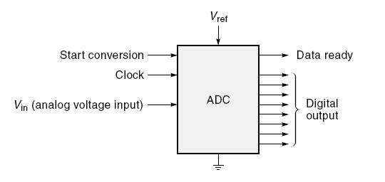
Analog-to-digital conversion is a more complicated process (than for the DAC), and the hardware requires some conversion time, which is typically in the microsecond range. The conversion time required depends on the type of ADC, the applied clock frequency, and the number of bits being converted. Figure shows a block diagram for an 8-bit ADC. The input Vin can be any voltage between 0 V and Vref. When Vin is 0 Vdc, the output is 00000000; when Vin is Vref, the output is 11111111 (255 decimal).
For input voltages between 0 and Vref, the output increases linearly with Vin; therefore, we can develop a simple ratio for the ADC:
output = decimal output value of an 8-bit ADC
Vin = analog input voltage to the ADC
Vref = ADC reference voltage
To start the conversion process, a start-conversion pulse is sent to the ADC. The ADC then samples the analog input and converts it to binary. When completed, the ADC activates the data-ready output. This signal can be used to alert the computer to read in the binary data.
 Figure shows a data sheet for an 8-bit ADC (ADC0804). Packaged as a 20-pin DIP, this device can operate on a single 5-Vdc power supply and requires an external resistor and capacitor to complete the ADC circuit. The start-conversion pulse is applied to pin 3 (WR), and the data-ready signal comes from pin 5 (INTR). This particular ADC can be connected in a free-running mode where it performs one conversion after the other as fast as it can. Notice also that the pin labeled Vref/2 (pin 9) must be set at half of the actual Vref. For example, if the requirements call for an analog voltage range of 0-5 Vdc, then pin 9 would be set to 2.5 Vdc. The time to complete a conversion is approximately 100 µs (micro-seconds), making it almost 700 times slower than the DAC0808 discussed earlier.
Tags:-analog-to-digital converter,adc datasheet,adc design,adc0804,Australian dental council,adc0808,active directory connector,active desktop calendar,adc0804 datasheet,adc0808,adc0804 pdf,adc0804lcn,lm35,Dac0800,dac0808,adc0809,interfacing adc 8051,adc0808 interfacing with 8051,ADC Example Code mbed - Rapid Prototyping for Microcontrollers,8051 with microcontrollers tutorial,adc interfacing projects,adc0804 interfacing 8051
BACK to Content Page
.
Next Page
.
Previous Page
The output of the pressure transducer is an analog signal .To interface with the microcontroller it is needed to change this signal in to digital value because the microcontroller and other digital devices works on the digital data . For this purpose ADC is used. We used an IC(ADC0804) which gave an 8 bit digital value for the input analog valued signal.
Analog signals are very common inputs to embedded systems – Most transducers and sensors are analog. Special devices needed to interface the analog systems to digital systems. ADC (Analog to Digital Converter) is used between signal input and the embedded system. DAC (Digital to Analog Converter) between embedded system and analog signal output
An analog-to-digital converter (ADC) is a circuit that converts an analog voltage into a digital word. A typical ADC consists of a single IC with a few support components.
Analog-to-digital conversion is a more complicated process (than for the DAC), and the hardware requires some conversion time, which is typically in the microsecond range. The conversion time required depends on the type of ADC, the applied clock frequency, and the number of bits being converted. Figure shows a block diagram for an 8-bit ADC. The input Vin can be any voltage between 0 V and Vref. When Vin is 0 Vdc, the output is 00000000; when Vin is Vref, the output is 11111111 (255 decimal).
For input voltages between 0 and Vref, the output increases linearly with Vin; therefore, we can develop a simple ratio for the ADC:
Solving for output gives the following:

whereoutput = decimal output value of an 8-bit ADC
Vin = analog input voltage to the ADC
Vref = ADC reference voltage
To start the conversion process, a start-conversion pulse is sent to the ADC. The ADC then samples the analog input and converts it to binary. When completed, the ADC activates the data-ready output. This signal can be used to alert the computer to read in the binary data.
Tags:-analog-to-digital converter,adc datasheet,adc design,adc0804,Australian dental council,adc0808,active directory connector,active desktop calendar,adc0804 datasheet,adc0808,adc0804 pdf,adc0804lcn,lm35,Dac0800,dac0808,adc0809,interfacing adc 8051,adc0808 interfacing with 8051,ADC Example Code mbed - Rapid Prototyping for Microcontrollers,8051 with microcontrollers tutorial,adc interfacing projects,adc0804 interfacing 8051
BACK to Content Page
.
Next Page
.
Previous Page


No comments:
Post a Comment