Monday, October 24, 2011

Control Cascade Control Systems Design - Tunings

Procedure for Cascade Control Systems Design:
Choice of Suitable
PID TuningsAbstract: This paper provides an approach for the application of PID controllers
within a cascade control system configuration. Based on considerations about the
expected operating modes of both controllers, the tuning of both inner and outer loop
controllers are selected accordingly. This fact motivates the use of a tuning that,
for the secondary controller, provides a balanced set-point / load-disturbance performance.
A new approach is also provided for the assimilation of the inner closed-loop
transfer function to a suitable form for tuning of the outer controller. Due to the fact
that this inevitably introduces unmodelled dynamics into the design of the primary
controller, a robust tuning is needed.

2 Cascade Control


3 g-tuning for balanced Servo/Regulation
4 Approach for Cascade Control Design
4.1 Inner loop and outer loop process models
4.2 Inner loop controller tuning
Set-point tuning settings
Load-disturbance tuning settings
4.3 Model for Outer loop tuning
4.4 Outer loop controller tuning
5 Equivalent model approximation
6 Example
7 Conclusions
http://www.journal.univagora.ro/download/pdf/134.pdf

How to Tune Cascade Loops
1 An overview of Cascade Control.
What's The Inner Loop For?
• Reduces phase lag of inner process
• Disturbances to the inner loop are
compensated for before they upset the
outer loop
• Prevents non-linearities in the inner loop
from reaching the outer loop

2 Tuning Cascade Control Loops.
What happens when cascade loops
are poorly tuned?
• Loops “fight” each other
• Create oscillations
• Neither variable is properly controlled
• Operator puts loop in manual.
Tuning Cascade Loops
1. Always check for measurement and
valve-related issues.
2. Inner Loop Tuning - put slave into
Local Auto or Manual and tune the
slave controller as a normal PID loop.
3. Outer Loop Tuning - put slave into
Cascade and tune master controller
as a normal PID loop.
4. Adjust outer loop tuning values to
ensure that the RRT (Relative
Response Time) of outer loop is 3-5
times slower than the inner loop.

3 Case Study.

http://www.expertune.com/articles/UG2007/CascadeTuning.pdf

Cascade Control
Handle Processes that Challenge Regular PID Control


In previous columns we have named lags in a process as major obstacles to good temperature control. When they are inconveniently long and come in multiple stages, first try to determine where changes to process design can avoid or reduce lags. Then do your best with PID control and if you fail to obtain the response you hoped for you can turn to cascade control.


Tuning.Tune the slave loop first. Set TC1 to manual. Remove integral and derivative action from TC2 and tune it aiming for tight control. Absence of derivative avoids excessive activity of the slave loop. Overall integral action to remove offset in the vessel temperature is already provided by the master controller.


When tuning the master loop, return to cascade control, remove derivative action and tune in the normal way. Note that the slave loop now becomes part of the master loop that you are tuning at TC1. Bumpless transfer between auto, manual and cascade will be a standard feature of TC1.
Set point limits on the slave loop. If you know the range of TC2 (fluid) temperatures needed to hold the vessel temperature under all expected conditions, put those values as limits on the set point of TC2.

http://www.pacontrol.com/download/Cascade%20Control%20-%20Handle%20Processes%20that%20Challenge%20Regular%20PID%20Control.pdf


Cascade Controller - Auto Tuning

Relay Auto Tuning Of Parallel Cascade Controller
Abstract
The present work is concerned with relay auto tuning of
parallel cascade controllers. The method proposed by
Srinivasan and Chidambaram [10] to analyze the conventional
on-off relay oscillations for a single loop feedback controller is
extended to the relay tuning of parallel cascade controllers.
Using the ultimate gain and ultimate cross over frequency of
the two loops, the inner loop (PI) and outer loop (PID)
controllers are designed by Ziegler-Nichols tuning method. The
performances of the controllers are compared with the results
based on conventional relay analysis. The improved method of
analyzing biased auto tune method proposed for single
feedback controller by Srinivasan and Chidambaram [11] is
also applied to relay auto tune of parallel cascade controllers.
The proposed methods give an improved performance over that
of the conventional on-off relay tune method.

http://www.iaeng.org/publication/WCECS2007/WCECS2007_pp158-162.pdf
read more "Control Cascade Control Systems Design - Tunings"

Thursday, October 20, 2011

Control Temperature Indicator Circuit

This circuit uses a Dallas DS1621 temperature sensor which indicates the temperature of the device. The temperature sensor has a thermal alarm output, which becomes high when the temperature of the device exceeds a user defined value. This is the figure of the circuit.


When the temperature drops below a user defined value, the alarm output becomes low. In this way any amount of hysteresis can be programmed. The values are stored in a special register of the device that is nonvolatile. The signal of the alarm output is amplified by a BC557 PNP transistor, that is drives a relay that can switch a heater element or a blower on or off. The temperature settings and readings are communicated to/from the device over a simple 2-wire serial interface. An ATMEL 90S2313 microcontroller controls the serial communication to/from the DS1621.The microcontroller also controls three LED, only one of the LED's is on when the temperature is within a certain range. The range of the temperature in which the LED's are on can be set by the user in the program code. The circuit needs to be powered by a 5V power supply, which can be obtained from a wall-wart.

read more "Control Temperature Indicator Circuit"

Control Analog to Digital Converter (ADC) Circuit Using ATmega8

An analog to digital converter converts an analog input voltage into a digital value. This is a circuit for shows the analog to digital converter. This circuit is using microcontroller ATmega8 for control the operation. This is the figure of the circuit.


The resolution of the converter indicates the number of discrete values it can produce. It is usually expressed in bits. For example, an ADC that encodes an analog input to one of 256 discrete values has a resolution of eight bits, 28 = 256. Most ADCs are linear, which means that they are designed to produce an output value that is a linear function of, i.e. proportional to, the input. In this circuit, Atmega8 has 6 AD-converters which have a resolution of 10 bits so it has 210 = 1024 discrete values. In his example a potentiometer is connected to the portC.0 of the Mega8 and a LCD module of 20x4 characters is connected to port D. The LCD module displays the values that are measured on the ADC port. The values are presented on the display as discrete values (0 to 1023), the percentage (0 to 100%) of the values and in a bargraph display.
read more "Control Analog to Digital Converter (ADC) Circuit Using ATmega8"

Wednesday, October 19, 2011

Control Light Sensor Circuit Using Programmable Gain Amplifier

This light sensor circuit that is photos sensor is the gap between light and electronics. This circuit is built by op amp and microcontroller PIC16C63 for control the sensor. This circuit is not precision application, but they can be effectively used in position photo sensing applications minus the headaches of amplifier stability. This is the figure of the circuit.


When the two, six or eight channel PGA is used in this system, the other channels can be used for other sensors or an array of photo sensors without an increase in signal conditioning hardware or PIC micro® microcontroller I/O pin consumption. The multiplexer and high-speed conversion response of the PGA / Analog-to-Digital (A/D) conversion allows the photo sensor input signal to be sampled and quickly converted to the digital domain. Switching from channel to channel is then easier with the Serial Peripheral Interface (SPI) from the PIC16C63 microcontroller to the PGA. The PGA can be configured with a photo sensor in two different settings. These circuits are appropriate for signal responses from DC to ~100 KHz. [Schematic circuit source: Microchip Technology, Inc]

read more "Control Light Sensor Circuit Using Programmable Gain Amplifier"

Control Air Flow Sensor Circuit Using PIC16C781

This circuit is describes about sensing air flow using microcontroller PIC16C781. In this circuit is using Programmable Switch Mode Controllers (PSMC) that combination between the Integrated Operational Amplifier, Digital-to-Analog Converter (DAC), and gated timer to construct a thermally operated air flow sensor with minimum external components. This is the figure of the circuit.


Air flow is detected by the cooling effect of air movement across a heated resistor. R5 and R7 are thin film platinum Resistance Temperature Detectors (RTD). These are essentially thermistor with a very linear temperature response. The flow sensor is comprised of R6 and R7. Changes in ambient temperature conditions are compensated by two voltage dividers, R2-R5 and R1-R7. R2 and R5 form a voltage divider between the Op Amp output and the Op Amp inverting input. Similarly, R1 and R7 form a voltage divider between the variable DAC reference and the non-inverting Op Amp input. Since R5 and R7 are identical RTD's, resistance variations due to self heating, as well as changes in the ambient conditions, cancel out at the Op Amp inputs.

This technical brief demonstrates how temperature changes resulting in milliohm differences can be measured quickly and accurately using only the built-in peripherals of the PIC16C781. This is the first of the mixed-signal PICmicro® microcontrollers with integral DAC, operational amplifier, comparators, PSMC and gated timer inputs which, when used in harmony, make such measurements possible. [Schematic source: Microchip Technology Inc].
read more "Control Air Flow Sensor Circuit Using PIC16C781"

Saturday, October 15, 2011

Schematic Seven Segment Displays of Pressure Monitoring Project

A seven-segment display is an integrated circuit package with seven light emitting diodes (LEDs) in it. The seven segments (LEDs) are arranged in a figure eight and given the standard letter designations a-g as shown in the figure below. The way to remember the letters is that they start at the top, increase clockwise ,and the crossbar is last.

Many seven-segment displays also have an eighth LED for a decimal point. This LED is often labeled RHP (for right-hand point) or LHP (for left-hand point) on pin-out diagrams. On RHP displays the decimal point is to the right of the figure 20 and on LHP displays to the left. Diodes (including light-emitting diodes) have two terminals called the anode and the cathode. The LED lights when the diode is forward biased, which occurs when the anode is at higher voltage than the cathode. The LED does not light when the anode and cathode are at the same voltage or if the LED is reversed biased (anode at lower voltage than cathode).

Since the seven-segment display contains seven diodes we would expect that there would be 14 pins corresponding to seven anodes and seven cathodes (16pins if there is a decimal point). However actual seven-segment displays almost always have a common terminal. A common-anode display has the anode terminals of every LED tied together internally. A common-cathode display has the cathode of every LED tied together internally. All of the LEDs in the project are common anode. Common-anode LEDs are more convenient to use since they can be driven by open-collector devices whereas common-cathode LEDs can not. A diagram of the pin-out of a common-anode seven segment display is shown in the figure below. Notice that there are often two internally-connected common pins that help with current-carrying capacity. There would be nine pins on this package (2 commons and the 7 pins for the a-g cathodes).


To make the 7-segment display active, we need to connect the common-anode pins to high voltage. The individual segments may now be lit by connecting the individual cathodes to ground or not lit by connecting the cathode to either the high voltage of by letting it float. One problem is that the LEDs will use to much power and possibly burn out if connected directly across a 5V power supply. To reduce power consumption and protect the diodes from damage, we use a current-limiting resistor. A 330Ω resistor will work well in this lab (220Ω and 470Ω are also reasonable). This will keep the current in each LED down to about 10-15 milliamps (mA). The figure below shows the use of seven current-limiting resistors with a common-anode display which is always enabled. The pin-out for the 7-segment display is normally as shown below. Notice that there are places where you would expect pins but there are no pins on the display package. Also, depending on which display is used, either RHP, LHP, or both may not be implemented.
Tags:- seven segment data sheet,seven segment display datasheet,seven segment display interfacing,seven segment display decoder,seven segment display circuits,seven segment datasheet,seven segment led digit delphi,seven segment digital clock


 BACK to Content Page

 .

 Next Page
.
   Previous Page
read more "Schematic Seven Segment Displays of Pressure Monitoring Project"

Schematic SN74LS373 Latch with 3-State Outputs and interface with microcontroller

The SN74LS373 consists of eight latches with 3-state outputs for bus organized system applications. The flip-flops appear transparent to the data (data changes asynchronously) when Latch Enable (LE) is HIGH. When LE is LOW, the data that meets the setup times is latched. Data appears on the bus when the Output Enable (OE) is LOW. When OE is HIGH the bus output is in the high impedance state.

The SN74LS374 is a high-speed, low-power Octal D-type Flip-Flop featuring separate D-type inputs for each flip-flop and 3-state outputs for bus oriented applications. A buffered Clock (CP) and Output Enable (OE) is common to all flip-flops. The SN74LS374 is manufactured using advanced Low Power Schottky technology and is compatible with all ON Semiconductor TTL families.


Some features of octal D-type Flip-Flop with 3-State Output
• Eight Latches in a Single Package.
• 3-State Outputs for Bus Interfacing.
• Hysteresis on Latch Enable.
• Edge-Triggered D-Type Inputs.
• Buffered Positive Edge-Triggered Clock.
• Hysteresis on Clock Input to Improve Noise Margin.
• Input Clamp Diodes Limit High Speed Termination Effects


 BACK to Content Page
.
 Next Page
 .
   Previous Page
used urological ultrasound with transrectal probe cyprus circuit diagram of piezoelectric sensor based heart beat monitor 16f877a frequency counter software free download c language microcontroller projects in c for 8051 full discription with circuit diagram max232 atmel programator rs232
read more "Schematic SN74LS373 Latch with 3-State Outputs and interface with microcontroller"

Thursday, October 13, 2011

Control PID Controllers Auto Tuning - Relay Feedback

Relay Feedback Auto Tuning of PID Controllers

IntroductionFor a certain class of process plants, the so-called \auto tuning" procedure
for the automatic tuning of PID controllers can be used. Such a procedure
is based on the idea of using an on/off controller (called a relay controller)
whose dynamic behaviour resembles to that shown in Figure 1(a). Starting
from its nominal bias value (denoted as 0 in the Figure) the control action
is increased by an amount denoted by h and later on decreased until a value
denoted by -h.


The closed-loop response of the plant, subject to the above described ac-
tions of the relay controller, will be similar to that depicted in Figure 1(b).
Initially, the plant oscillates without a de¯nite pattern around the nominal
output value (denoted as 0 in the Figure) until a de¯nite and repeated out-
put response can be easily identi¯ed. When we reach this closed-loop plant
response pattern the oscillation period (Pu) and the amplitude (A) of the
plant response can be measured and used for PID controller tuning. In fact,
the ultimate gain can be computed as:
Having determined the ultimate gain Kcu and the oscillation period Pu
the PID controller tuning parameters can be obtained from the following
table:
Example of Relay Feedback Auto Tuning of PID Controllers

http://200.13.98.241/~antonio/cursos/control/notas/siso/atv.pdf
Relay-based PID Tuning
ABSTRACT

Relay-based auto tuning is a simple way to tune PID controllers
that avoids trial and error, and minimises the possibility
of operating the plant close to the stability limit.


http://homepages.ihug.co.nz/~deblight/AUTResearch/papers/relay_autot.pdf


An Improved Relay Auto Tuning of PID Controllers for SOPTD
Systems


Difficulties of loop tuning
When you discuss loop tuning with instrument and control
engineers, conversation soon turns to the Zeigler-Nichols
(ZN) ultimate oscillation method. Invariably the plant engineer
soon responds with ‘Oh yes, I remember the ZN tuning
scheme, we tried that and the plant oscillated itself into
oblivion — bad strategy. Moreover when it did work, the
responses are overly oscillatory’
So given the tedious and possibly dangerous plant trials
that result in poorly damped responses, it behoves one to
speculate why it is often the only tuning scheme many instrument
engineers are familiar with, or indeed ask if it has
any concrete redeeming features at all.
In fact the ZN tuning scheme, where the controller gain
is experimentally determined to just bring the plant to the
brink of instability is a form of model identification. All
tuning schemes contain a model identification component,
but the more popular ones just streamline and disguise that
part better. The entire tedious procedure of trial and error
is simply to establish the value of the gain that introduces
half a cycle delay when operating under feedback. This is
known as the ultimate gain Ku and is related to the point
where the Nyquist curve of the plant in Fig. 1(b) first cuts
the real axis.

The problem is of course, is that we rarely have the luxury
of the Nyquist curve on the factory floor, hence the
experimentation required.
Abstract Using a single symmetric relay
feedback test, a method is proposed to identify
all the three parameters of a stable second order
plus time delay (SOPTD) model with equal time
constants. The conventional analysis of relay
auto-tune method gives 27% error in the
calculation of ku,. In the present work, a method
is proposed to explain the error in the ku
calculation by incorporating the higher order
harmonics. Three simulation examples are given.
The estimated model parameters are compared
with that of Li et al. [4] method and that of
Thyagarajan and Yu [8] method. The open loop
performance of the identified model is compared
with that of the actual system. The proposed
method gives performances close to that of the
actual system. Simulation results are also given
for a nonlinear bioreactor system. The open loop
performance of the model identified by the
proposed method gives a performance close to
that of the actual system and that of the locally
linearized model. SOPTD model, symmetric relay, auto-tuning


http://ntur.lib.ntu.edu.tw/bitstream/246246/87370/1/09.pdf

DEVELOPMENT OF AN AUTO-TUNING PID AND
APPLICATIONS TO THE PULP AND PAPER INDUSTRY
Abstract
An auto-tuning industrial PID is presented. The autotuning
is realized in three steps. The process is first
adequately excited in order to generate good quality data
for the second step, the process identification. The last step
is the PID tuning based on the evaluated parametric model.
The auto-tuning PID has been implemented on two
different control systems and successful applications to
processes of the pulp and paper industry are analyzed.


http://www.iaeng.org/publication/WCECS2007/WCECS2007_pp175-181.pdf

Auto-tune system using single-run relay feedback test
and model-based controller design
Abstract

In this paper, a systematic approach for auto-tune of PI/PID
controller is proposed. A single run of the relay feedback experiment
is carried out to characterize the dynamics including the type
of damping behavior, the ultimate gain, and ultimate frequency.
Then, according to the estimated damping behavior, the process
is classified into two groups. For each group of processes,
modelbased rules for controller tuning are derived in terms of
ultimate gains and ultimate frequencies. To classify the processes,
the estimation of an apparent deadtime is required. Two artificial
neural networks (ANNs) that characterize this apparent deadtime using
the ATV data are thus included to facilitate this estimation of
this apparent deadtime. The model-based design for this auto-tuning
makes uses of parametric models of FOPDT (i.e. first-order-plus-dead-time)
and of SOPDT (i.e. second-order-plus-dead-time)
dynamics. The results from simulations show that the controllers
thus tuned have satisfactory results compared with those from
other methods.

Tuning strategy for the model-based auto-tune system.


http://w3.gel.ulaval.ca/~desbiens/publications/DevelopmentOfAnAutoTuningPID.pdf

MODIFICATION AND APPLICATION OF AUTOTUNING
PID CONTROLLER

Abstract. This contribution presents a modified autotuning algorithm of the PID controller.
The motivation for the modification of the basic autotuning algorithm is to enlarge the class
of processes to which it can be applied. The basic autotuning algorithm introduced by
Åstrom and Hägglund is extended by the preliminary identification procedure and through
the usage of the dead time compensating controller. These modifications are detailed
through the description of the algorithms’ functioning. The proposed algorithm has been
implemented in the programmable logic controller (PLC) Siemens SIMATIC S7-300. The
experimental results confirm the good robustness properties of the proposed algorithm,
which were demonstrated in a simulation study.

Structure of the modified autotuning PID controller.


http://act.rasip.fer.hr/old/papers/MED00_062.PDF
read more "Control PID Controllers Auto Tuning - Relay Feedback"

Sunday, October 9, 2011

Control SPI Interface Circuit for Big 7 Segment LED

This circuit is uses for the general purpose Big LED with SPI serial interfacing. The circuit is using a serial-in-parallel out shift register, 74HC595 for receiving serial data from microcontroller board. This is the figure of the circuit.


For wiring the schematic is SER is for data input, SRCLK is shift clock and RCLK is Latch clock. Each data bit is shifted into the register on rising edge of the shift clock. When all data bits are shifted into the 8-bit register, the rising edge of RCLK will clock the data to be latched at each output bit, i.e. QA - QH. The Big LED is made from cheap dot LED. Each segment has five dot LED connected in series with a limiting resistor tied to +12V. The logic high at the input of ULN2003 makes the output active low, thus sinks the LED current into the chip. The driver has 7-bit for segment a, b, c, d, e, f, and g. Q1 is for optional point display.

Multiple digits can easily be made by connecting the QH to the next digit serial input bit, see the circuit below. Please note that, the shift clock and latch signal are tied to every 74HC595.


read more "Control SPI Interface Circuit for Big 7 Segment LED"

Tuesday, October 4, 2011

Schematic Use of MICROCONTROLLER in Pressure Monitoring Project

The ATMEL Microcontroller AT89C51
The 89C51 is an 8-bit microprocessor originally designed in the 1980's by Intel that has gained great popularity since its introduction. Its standard form includes several standard on-chip peripherals, including timers, counters, and UART's, plus 4kbytes of on-chip program memory and 128 bytes (note: bytes, not Kbytes) of data memory, making single-chip implementations possible. Its hundreds of derivatives, manufactured by several different companies (like Philips) include even more on-chip peripherals, such as analog-digital converters, pulse-width modulators, I2C bus interfaces, etc. Costing only a few dollars per IC, the 8051 is estimated to be used in a large percentage (maybe 1/2?) all embedded system products.

Some features of the 8051 Micrcontroller are.
• 89C51 Central Processing Unit.
• On-chip FLASH Program Memory.
• Speed up to 33 MHz.
• Fully static operation.
• RAM expandable externally up to 64 kbytes.
• 4 interrupt priority levels.
• 6 interrupt sources.
• Four 8-bit I/O ports.
• Full-duplex enhanced UART.
• Framing error detection.
• Automatic address recognition.
• Three 16-bit timers/counters T0, T1 (standard 80C51) and additional T2 (capture and compare) Power control modes.
• In microcontroller 8051 Clock can be stopped and resumed.
• Idle mode.
• The microcontroller 8051 has Power down mode.
• Programmable clock out.
• Second DPTR register.
• Asynchronous port reset.
• Low EMI (inhibit ALE) .
• Wake up from power down by an external interrupt

The Microcontroller 8051 memory architecture includes 128 bytes of data memory that are accessible directly by its instructions. A 32-byte segment of this 128 byte memory block is bit addressable by a subset of the 8051 instructions, namely the bit-instructions.With Microcontroller 8051 External memory of up to 64 Kbytes is accessible by a special "movx" instruction. Up to 4 Kbytes of program instructions can be stored in the internal memory of the 8051, or the 8051 can be configured to use up to 64 Kbytes of external program memory The majority of the 8051's instructions are executed within 12 clock cycles.

OSCILLATOR CHARACTERISTICS:

XTAL1 and XTAL2 are the input and output, respectively, of an inverting amplifier. The pins can be configured for use as on-chip oscillator. To drive the device from an external clock source, XTAL1 should be driven while XTAL2 is left unconnected. There are no requirements on the duty cycle of the external clock signal, because the input to the internal clock circuitry is through a divide-by-two flip-flop. However, minimum and maximum high and low times specified in the data sheet must be observed.
 RESET:
A reset is accomplished by holding the RST pin high for at least two machine cycles (24 oscillator periods), while the oscillator is running. To insure a good power-on reset, the RST pin must be high long enough to allow the oscillator time to start up (normally a few milliseconds) plus two machine cycles. At power-on, the voltage on VCC and RST must come up at the same time for a proper start-up. Ports 1, 2, and 3 will asynchronously be driven to their reset condition when a voltage above VIH1 (min.) is applied to RST. The value on the EA pin is latched when RST is de-asserted and has no further effect.

 BACK to Content Page
 .
 Next Page
.
   Previous Page
read more "Schematic Use of MICROCONTROLLER in Pressure Monitoring Project"

Schematic PERIPHERAL INTERFACE IN THE PROJECT OF PRESSURE MONITORING

As we know that the 8051 microcontroller has 4 ports. Sometimes when we want to interface more devices with microcontroller, these four ports becomes not sufficient and we feel requirement for more i/o lines. In this project we do the practice to increase the number of i/o lines or i/o ports of microcontroller 8051.
The number of ports available can be increased using a peripheral interface like 8255 PPI , and like that.

 8255 the Programmable Peripheral Interface
The Intel 8255 (or i8255) Programmable Peripheral Interface chip is a peripheral chip originally developed for the Intel 8085 microprocessor. The 8255 Programmable Peripheral Interface (PPI) is a versatile and easy to construct circuit card the plugs into an available slot in your IBM PC. The 8255 Programmable Peripheral Interface (PPI) is a very popular and versatile input / output chip that is easily configured to function in several . The use of 8255 PPI to increase the i/o lines of microcontroller 8051 is a good option. Here we discuss it in some detail, the hardware and software requirements of the interface of 8255 PPI.
how a PC printer port may be interfaced with an 8255 Programmable Peripheral Interface to provide 24 outputs.
Pin Configuration
D0 - D7 These are the data input/output lines for the device. All information read from and written to the 8255 occurs via these 8 data lines.
CS (Chip Select Input). If this line is a logical 0, the microprocessor can read and write to the8255.
RD (Read Input) Whenever this input line is a logical 0 and the RD input is a logical 0, the 8255 data outputs are enabled onto the system data bus.
WR (Write Input) Whenever this input line is a logical 0 and the CS input is a logical 0, data is written to the 8255 from the system data bus
A0 - A1 (Address Inputs) The logical combination of these two input lines determines which internal register of the 8255 data is written to or read from.
RESET. The 8255 is placed into its reset state if this input line is a logical 1. All peripheral ports are set to the input mode.
PA0 - PA7, PB0 - PB7, PC0 - PC7 These signal lines are used as 8-bit I/O ports. They can be connected to peripheral devices. The 8255 has three 8 bit I/O ports and each one can be connected to the physical lines of an external device. These lines are labeled PA0-PA7, PB0-PB7, and PC0-PC7. The groups of the signals are divided into three different I/O ports labeled port A (PA), port B (PB), and port C (PC).

 Control Modes
The 8255 allows for three distinct operating modes (Modes 0, 1 and 2) as follows.
Mode 0
Ports A and B operate as either inputs or outputs and Port C is divided into two 4-bit groups either of which can be operated as inputs or outputs
 Mode 1
Same as Mode 0 but Port C is used for handshaking and control
 Mode 2
Port A is bidirectional (both input and output) and Port C is used for handshaking. Port B is not used.
RS232
8051 microcontroller represents ‘1’ by +5 volts and ’0’ by 0 volts while a computer represents ‘1’ by and a zero by. To make the output of a microcontroller compatible with the pc RS232 is used. Now that we have the 8 bit value in the 8051, we want to send that value to the PC. The 8051 has a built in serial port that makes it very easy to communicate with the PC's serial port but the 8051 outputs are 0 and 5 volts and we need +10 and -10 volts to meet the RS232 serial port standard. The easiest way to get these values is to use the MAX232. The MAX232 acts as a buffer driver for the processor. It accepts the standard digital logic values of 0 and 5 volts and converts them to the RS232 standard of +10 and -10 volts. It also helps protect the processor from possible damage from static that may come from people handling the serial port connectors.
The MAX232 requires 5 external 1uF capacitors. These are used by the internal charge pump to create +10 volts and -10 volts. For the first capacitor, the negative leg goes to ground and the positive leg goes to pin 16. For the second capacitor, the negative leg goes to 5 volts and the positive leg goes to pin 2. For the third capacitor, the negative leg goes to pin 3 and the positive leg goes to pin 1. For the fourth capacitor, the negative leg goes to pin 5 and the positive leg goes to pin 4. For the fifth capacitor, the negative leg goes to pin 6 and the positive leg goes to ground. The MAX232 includes 2 receivers and 2 transmitters so two serial ports can be used with a single chip. We will only use one transmitter for this project. The only connection that must be made to the 8051 is one jumper from pin 3 of the 8051 to pin 11 of the MAX232. To power the MAX232, Connect pin 16 to 5 volts and 15 to ground. The only thing left is that we need some sort of connector to connect to the serial port. The sample code below is written for Comm1 and most computers use a 9 pin DB9 male connector for Comm1 so a 9 pin female connector is included for this project. You may also want to buy a DB9 extension cable (Shown on order form as DB9 to DB9 cable) to make the connection easier. There should be 3 wires soldered to the DB9 connector pins 2, 3 and 5. Connect the wire from pin 5 of the connector to ground on the breadboard. Connect the wire from pin 2 of the connector to pin 14 of the MAX232. (The other wire is for receiving and is not used in this project.)


 BACK to Content Page
.
Next Page
.
   Previous Page
Tags:
interface in a microcontroller based system,sixteen leds are connected to port pnn and sixteen switches are connected to port pmm,8255 Programmable Peripheral Interface Pinout; Block diagram; BSR mode; I/O mode; Mode 1; Mode 2,The Intel 8255 (or i8255) Programmable Peripheral Interface chip is a peripheral chip originally developed for the Intel 8085 microprocessor, The 8255A is a programmable peripheral interface (PPI) device designed for use in Intel mic systems. Its function is that of a general purposes I/O expander,8255 Programmable Peripheral Interface (PPI). Data Bus Buffer. This three-state bi-directional 8-bit buffer is used to interface the 8255 to the system data ,Address decoding; Interface with memory; Introduction to Programmable Peripheral,8255 PROGRAMMABLE PERIPHERAL INTERFACE. 8255 is a widely used programmable parallel I/O device. This is also named as programmable peripheral input output device,8255 programmable peripheral interface Free 8085 Microprocessor Based projects with source code and circuit diagram.The 8255A programmable peripheral interface (PPI) implements a general-purpose. I/O interface to connect peripheral equipment to a microcomputer system bus. 8255 programmable peripheral interface to interface I/O devices with 8085 as it only has 3 ports,82C55A. CMOS Programmable. Peripheral Interface. Features. • Pin Compatible with NMOS 8255A. • 24 Programmable I/O Pins. • Fully TTL Compatible,8255A/8255A-5. 8255A FUNCTIONAL DESCRIPTION. General. The 8255A is a programmable peripheral interface. (PPI) device designed for use in Intel microcomputer ,8051 Microcontroller Projects AVR PIC Projects Tutorials Ebooks Libraries codes PPI POrt expander,port extension
read more "Schematic PERIPHERAL INTERFACE IN THE PROJECT OF PRESSURE MONITORING"

Monday, October 3, 2011

Schematic Analog to Digital Conversion process in Pressure Monitoring Project

Analog to Digital Conversion process in 8051 Microcontroller Based Pressure Monitoring Project:-
The output of the pressure transducer is an analog signal .To interface with the microcontroller it is needed to change this signal in to digital value because the microcontroller and other digital devices works on the digital data . For this purpose ADC is used. We used an IC(ADC0804) which gave an 8 bit digital value for the input analog valued signal.
Analog signals are very common inputs to embedded systems – Most transducers and sensors are analog. Special devices needed to interface the analog systems to digital systems. ADC (Analog to Digital Converter) is used between signal input and the embedded system. DAC (Digital to Analog Converter) between embedded system and analog signal output
An analog-to-digital converter (ADC) is a circuit that converts an analog voltage into a digital word. A typical ADC consists of a single IC with a few support components.
Analog-to-digital conversion is a more complicated process (than for the DAC), and the hardware requires some conversion time, which is typically in the microsecond range. The conversion time required depends on the type of ADC, the applied clock frequency, and the number of bits being converted. Figure  shows a block diagram for an 8-bit ADC. The input Vin can be any voltage between 0 V and Vref. When Vin is 0 Vdc, the output is 00000000; when Vin is Vref, the output is 11111111 (255 decimal).
For input voltages between 0 and Vref, the output increases linearly with Vin; therefore, we can develop a simple ratio for the ADC:
Solving for output gives the following:

where
output = decimal output value of an 8-bit ADC
Vin = analog input voltage to the ADC
Vref = ADC reference voltage
To start the conversion process, a start-conversion pulse is sent to the ADC. The ADC then samples the analog input and converts it to binary. When completed, the ADC activates the data-ready output. This signal can be used to alert the computer to read in the binary data.

Figure  shows a data sheet for an 8-bit ADC (ADC0804). Packaged as a 20-pin DIP, this device can operate on a single 5-Vdc power supply and requires an external resistor and capacitor to complete the ADC circuit. The start-conversion pulse is applied to pin 3 (WR), and the data-ready signal comes from pin 5 (INTR). This particular ADC can be connected in a free-running mode where it performs one conversion after the other as fast as it can. Notice also that the pin labeled Vref/2 (pin 9) must be set at half of the actual Vref. For example, if the requirements call for an analog voltage range of 0-5 Vdc, then pin 9 would be set to 2.5 Vdc. The time to complete a conversion is approximately 100 µs (micro-seconds), making it almost 700 times slower than the DAC0808 discussed earlier.
Tags:-analog-to-digital converter,adc datasheet,adc design,adc0804,Australian dental council,adc0808,active directory connector,active desktop calendar,adc0804 datasheet,adc0808,adc0804 pdf,adc0804lcn,lm35,Dac0800,dac0808,adc0809,interfacing adc 8051,adc0808 interfacing with 8051,ADC Example Code mbed - Rapid Prototyping for Microcontrollers,8051 with microcontrollers tutorial,adc interfacing projects,adc0804 interfacing 8051


 BACK to Content Page
 .
 Next Page
 .
   Previous Page
read more "Schematic Analog to Digital Conversion process in Pressure Monitoring Project"

Schematic Designing pressure transducer

 Designing pressure transducer for the project of Monitoring Pressure in Process industry.

As clear from the name, it is a device that that transforms the input pressure in to an electrical signal, which tells the magnitude of the input pressure and changes its value with the change in the input pressure.Pressure sensors can vary drastically in technology, design, performance, application suitability and cost. New pressure sensors combine silicon technology and analogue circuitry with modular design and lean manufacturing techniques.Most pressure transducers in use today use the same basic analog design circuitry by measuring a low level signal, amplifying and filtering this signal.
It includes the following parts:

• Cylinder and piston
• Spring
• Damper
• Displacement sensing machanism

 Cylinder and Piston
A specially designed cylinder and piston setup is used for the sake of acquiring the pressure from the pressurized system. Pressure is exerted on the piston and piston moves along the direction of the force applied by the pressure. Motion of the piston is limited by the attached spring and the damper. Design methodologies and techniques for creating robust sensor designs for automotive applications.

Displacement sensing mechanism
This setup is responsible for calculation of the displacement the piston has moved. It works on the principle of linear variable resistor. This resistor is attached with the piston. As the piston moves the resistance in the variable resisteor changes causing ht echange in the voltage level. This change in voltage level is of continuous level. This continuous level voltage is conveyed to the ADC fort the conversion it to the discrete levels

Linear variable resistor
This resistor is designed by the team. It includes the only a single rod of the graphite. current-to-pressure transducer is sensitive to shock, vibration, and position change.High accuracy and reliability; Completely submersible pressure transducer and cable; Compact, rugged design for easy installation; Minimal maintenance.The design, construction and performance of the Digiquartz Pressure Transducers are described.


Properties of graphite
Graphite is allotrope of the carbon. Its partially conducting material so its resistance changes as the length of the rod changes. It helped to design a proper variable potentiodivider.

 Spring
Spring is of spring constant Ks. this is the main functional unit that is responsible for the all sensing the pressure. Pressure exerts the force on the piston. Its displacement can be obtained from the linear variable resistor. Then the displacement is converted into the force that the air or any fluid exerts on the piston.

Damper
This damper is used to avoid any pressure surge and the piston moves slowly and adapts the level of the pressure.

Tags:- sensors such as a pressure sensor, pressure transducer or proximity,Custom Sensor Design,pressure sensors and pressure transducers, design Custom Load Cells, Custom Torque Sensors, and Custom Pressure Sensors, designing a strain gage pressure transducer, there are two fundamental considerations. One is the mechanical pressure-sensing element .
piezoelectric pressure sensor,to design a transducer specifically to measure melt pressure during the extrusion process ,How to develop pressure sensors,Pressure transducers, sensing element of pressure switch, industrial pressure sensors, home automation and control, Microcontroller 8051 based pressure sensing project, pressure monitoring based on microcontroller 8051, Algorithm to find pressure in a pipe, fluid pressure, fluid dynamics, flow sensor, interfacing of pressure transducers with microcontroller 8051, how can we measure pressure using microcontroller 8051. calculate pressure in the pipe, data logging and monitoring of pressure of pipe, computer aided pressure monitoring project, microcontroller and computer based data acquisition and control, industry automation using microcontroller, jigger machine pressure monitoring program, pressure jigger machine, how monitor high pressure with microcontroller, textile industry pressure monitoring project, cotton industry pressure monitoring project, microcontroller 8051 project to monitor pressure, velocity, flow rate height of fluid


  BACK to Content Page
.
 Next Page
 .
   Previous Page
read more "Schematic Designing pressure transducer"

Sunday, October 2, 2011

Schematic Types of Pressure sensor and transducer

3. Pressure sensor and transducer

3.1 Older ways to pressure measurement with Pressure gauges and switches


Mechanical methods of measuring pressure have been known for centuries. U-tube manometers were among the first pressure indicators. Originally, these tubes were made of glass, and scales were added to them as needed. But manometers are large, cumbersome, and not well suited for integration into automatic control loops. Therefore, manometers are usually found in the laboratory or used as local indicators. Depending on the reference pressure used, they could indicate absolute, gauge, and differential pressure.

pressure sensor and adc  Types of Pressure sensor and transducer
3.2 Advancement of Pressure sensors From Mechanical setup to Electronic setup

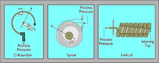
The first pressure gauges used flexible elements as sensors. As pressure changed, the flexible element moved, and this motion was used to rotate a pointer in front of a dial. In these mechanical pressure sensors, a Bourdon tube, a diaphragm, or a bellows element detected the process pressure and caused a corresponding movement.

a pressure sensor detects the pressure Types of Pressure sensor and transducer

microcontroller pressure sensor project Types of Pressure sensor and transducer
3.2.1 Transducer Types

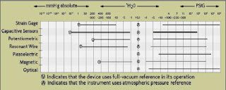
Figure provides an overall orientation to the scientist or engineer who might be faced with the task of selecting a pressure detector from among the many designs available. This table shows the ranges of pressures and vacuums that various sensor types are capable of detecting and the types of internal references (vacuum or atmospheric pressure) used, if any. Because electronic pressure transducers are of greatest utility for industrial and laboratory data acquisition and control applications, the operating principles and pros and cons of each of these is further elaborated in this section.
3.2.1.1 Capacitance

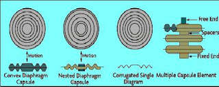
Capacitance pressure transducers were originally developed for use in low vacuum research. This capacitance change results from the movement of a diaphragm element (Figure ). The diaphragm is usually metal or metal-coated quartz and is exposed to the process pressure on one side and to the reference pressure on the other. Depending on the type of pressure, the capacitive transducer can be either an absolute, gauge, or differential pressure transducer.
3.2.1.2 Potentiometric

The potentiometric pressure sensor provides a simple method for obtaining an electronic output from a mechanical pressure gauge. The device consists of a precision potentiometer, whose wiper arm is mechanically linked to a Bourdon or bellows element. The movement of the wiper arm across the potentiometer converts the mechanically detected sensor deflection into a resistance measurement, using a Wheatstone bridge circuit (Figure )

Types of Pressure sensor and transducer,Pressure sensor interfacing with Microcontroller

  BACK to Content Page
 .
 Next Page  .

  Previous Page
Control Systems Projects in Industrial Electronics ,Wireless Pressure Sensors – Digital Pressure Sensor Transmitter,Energy Micro energy friendly ARM Cortex-M3 EFM32 microcontrollers extend an applications battery life , boost pressure sensor,Pressure sensor interfacing with Microcontroller,microcontroller pressure sensor project a pressure sensor detects the pressure,The HSCDANN001BA2A3 is a very accurate absolute pressure sensor from Honeywell, pressure sensor and adc ,8085/8086 Microprcessor and 8051 micro controller pressure sensor to microcontroller this project a barometric pressure sensor
read more "Schematic Types of Pressure sensor and transducer"