Wednesday, June 27, 2012

Control Free Microcontroller and Interface Programming 2010-06-27 08:36:00

Telephone Operated Remote Control Using PIC16F84A
This design controls up to 8 devices using a PIC microcontroller (PIC16F84A) connected to the phone line. The unique feature here is that unlike other telephone line based remote control, this device does not need the call to be answered at the remote end so the call will not be charged. This device depends on number of rings given on the telephone line to activate/deactivate devices. This is the figure of the circuit.


Instructions for the telephone operated remote switch:
A) While constructing the main circuit, make sure you use 18pin sockets (base) for the PIC16F84A. Do not solder the IC directly to the board since you may have to remove it for programming. Before you use the PIC on the main circuit, you have to first program it.
B) To program the PIC16F84A microcontroller:
C) Remove the PIC from the programmer socket and put it into the main circuit socket.
 Set the DIP SWITCH as follows:
Switch3   Switch4      No. of initial rings to Switch ON(activate half of the board)
OFF        OFF             5
ON         OFF             4
OFF        ON              3
ON         ON              2
The number of initial rings to Switch OFF is one more than the number of rings to switch ON. For example, if you have set switch3 OFF & Switch4 ON then number of initial rings to activate half of the board to switch ON the relays is 3 and number of initial rings to activate half of the board to switch OFF the relays is 3+1 = 4

Switch1  Swtich2        Delay before making the second set of rings
OFF        OFF             20sec
ON         OFF             15sec
OFF        ON              10sec
ON         ON              5sec
This is the maximum delay the board can take after it is half activated. It will reset after this delay.

D) Now connect the circuit to the phone line and switch on its power supply.
E) You can test the board now. For example set the DIP switch to Switch1 ON, Switch2 OFF (15 sec delay) & switch3 ON, switch4 OFF (4 rings to activate half for switching ON). If you want to switch ON relay 1 (connected to RB0 of main circuit) then you have to do the following:

1.    Give 4 rings and put down the receiver
2.    Wait 5 seconds (this 5 seconds wait is required to prevent the board from detecting continue rings)
3.    then within 15 seconds give 1 ring (1 ring for relay1, 2 rings for relay2 and so on) and put down the receiver
4.    then within 5 sec the relay1 will switch ON
To switch off relay1:
1.    Give 5 rings and put down the receiver
2.    Wait 5 seconds (this 5 seconds wait is required to prevent the board from detecting continous rings)
3.    then within 15 seconds give 1 ring (1 ring for relay1, 2 rings for relay2 and so on) and put down the receiver
4.    then within 5 sec the relay1 will switch OFF
read more "Control Free Microcontroller and Interface Programming 2010-06-27 08:36:00"

Control Decimal Vs Binary Numeration


Counting from zero to twenty using four different kinds of numeration systems: hash marks, Roman numerals, decimal, and binary:
System:    Hash Marks               Roman     Decimal     Binary
-------    ----------               -----     -------     ------
Zero       n/a                       n/a         0          0
One        |                          I          1          1
Two        ||                         II         2          10
Three      |||                        III        3          11
Four       ||||                       IV         4          100
Five       /|||/                      V          5          101
Six        /|||/ |                    VI         6          110
Seven      /|||/ ||                   VII        7          111
Eight      /|||/ |||                  VIII       8          1000
Nine       /|||/ ||||                 IX         9          1001
Ten        /|||/ /|||/                X          10         1010
Eleven     /|||/ /|||/ |              XI         11         1011
Twelve     /|||/ /|||/ ||             XII        12         1100
Thirteen   /|||/ /|||/ |||            XIII       13         1101
Fourteen   /|||/ /|||/ ||||           XIV        14         1110
Fifteen    /|||/ /|||/ /|||/          XV         15         1111
Sixteen    /|||/ /|||/ /|||/ |        XVI        16         10000
Seventeen  /|||/ /|||/ /|||/ ||       XVII       17         10001
Eighteen   /|||/ /|||/ /|||/ |||      XVIII      18         10010
Nineteen   /|||/ /|||/ /|||/ ||||     XIX        19         10011
Twenty     /|||/ /|||/ /|||/ /|||/    XX         20         10100

Neither hash marks nor the Roman system are very practical for symbolizing large numbers. Obviously, place-weighted systems such as decimal and binary are more efficient for the task. Notice, though, how much shorter decimal notation is over binary notation, for the same number of quantities. What takes five bits in binary notation only takes two digits in decimal notation. This raises an interesting question regarding different numeration systems: how large of a number can be represented with a limited number of cipher positions, or places? With the crude hash-mark system, the number of places IS the largest number that can be represented, since one hash mark "place" is required for every integer step. For place-weighted systems of numeration, however, the answer is found by taking base of the numeration system (10 for decimal, 2 for binary) and raising it to the power of the number of places. For example, 5 digits in a decimal numeration system can represent 100,000 different integer number values, from 0 to 99,999 (10 to the 5th power = 100,000). 8 bits in a binary numeration system can represent 256 different integer number values, from 0 to 11111111 (binary), or 0 to 255 (decimal), because 2 to the 8th power equals 256. With each additional place position to the number field, the capacity for representing numbers increases by a factor of the base (10 for decimal, 2 for binary).
An interesting footnote for this topic is the one of the first electronic digital computers, the Eniac. The designers of the Eniac chose to represent numbers in decimal form, digitally, using a series of circuits called "ring counters" instead of just going with the binary numeration system, in an effort to minimize the number of circuits required to represent and calculate very large numbers. This approach turned out to be counter-productive, and virtually all digital computers since then have been purely binary in design. To convert a number in binary numeration to its equivalent in decimal form, all you have to do is calculate the sum of all the products of bits with their respective place-weight constants. To illustrate:

Convert 110011012  to decimal form:
bits =         1  1  0  0  1  1  0  1           
.              -  -  -  -  -  -  -  -
weight =       1  6  3  1  8  4  2  1
(in decimal    2  4  2  6
notation)      8  

The bit on the far right side is called the Least Significant Bit (LSB), because it stands in the place of the lowest weight (the one's place). The bit on the far left side is called the Most Significant Bit (MSB), because it stands in the place of the highest weight (the one hundred twenty-eight's place). Remember, a bit value of "1" means that the respective place weight gets added to the total value, and a bit value of "0" means that the respective place weight does not get added to the total value. With the above example, we have:

12810  + 6410  + 810  + 410  + 110  = 20510

If we encounter a binary number with a dot (.), called a "binary point" instead of a decimal point, we follow the same procedure, realizing that each place weight to the right of the point is one-half the value of the one to the left of it (just as each place weight to the right of a decimal point is one-tenth the weight of the one to the left of it). For example:

Convert 101.0112  to decimal form:
.
bits =         1  0  1  .  0  1  1             
.              -  -  -  -  -  -  -
weight =       4  2  1     1  1  1 
(in decimal                /  /  /
notation)                  2  4  8

410  + 110  + 0.2510  + 0.12510  = 5.37510
read more "Control Decimal Vs Binary Numeration"

Saturday, June 23, 2012

Control Light Controller Using PIC 16F873


This circuit is a light controller with PIC 16F873. On this circuit, the control voltage is controlled by the variable resistor, and then by ADC on PIC16F873 converted to digital signals. To set the duration of the PWM pulse. This is the figure of the circuit;


This circuit is used to control the range of 100W.  Because the operating voltage of the PIC is 5 V, the transistor is used to control the 12V MOS FET.
read more "Control Light Controller Using PIC 16F873"

Tuesday, June 19, 2012

Schematic Signal control on ADC0804

In this section, we will discuss the practicle issues og ADC0804 and Signal control on ADC0804. Then we will move to the interfacing of ADC0804 with microcontroller.

Signal control on ADC0804

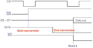
1. Make CS = 0 and send a L-to-H pulse to pin WR to start the conversion.
2. Keep monitoring the INTR pin. If INTR is low, the conversion is finished and we can go to the next step. If INTR is high, keep polling until it goes low.
3. After the INTR has become low, we make CS = 0 and send a H-to-L pulse to the RD pin to get the data out of the ADC0804 IC chip.

timing diagram of ADC0804
Note: CS is set to low for both RD and WR pulses.

Testing and interfacing of  ADC0804 microcontroller 8051

Write a program to monitor the INTR pin and bring the digital input value into register A. Then call a subroutine to display the input value on a 7-segment display. Do this continuously.
P2.6 = WR (Start conversion needs a L-to-H pulse)
; P2.7 = INTR (When low, end-of-conversion)
; P2.5 = RD (H-to-L will read the data from ADC chip)
; P1.0 – P1.7 = D0 – D7 of the ADC0804
;
MOV P1, #0FFH ; make P1=input
BACK: CLR P2.6 ; WR=0
SETB P2.6 ; WR=1 L-to-H to start conversion
HERE: JB P2.7, HERE ; wait for end of conversion
CLR P2.5 ; conversion finished, enable RD
MOV A, P1 ; read the data
ACALL DATA_DISPLAY ; display the data
SETB P2.5 ; make RD=1 for next round
SJMP BACK

Example of ADC Application

Temperature detection
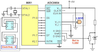
A temperature sensor (LM34 or LM35) is interfaced to the 8051 via an ADC (ADC0804)
The output voltage from the LM34/LM35 is linearly proportional to the measuring temperature
The ADC0804 converts the output voltages from the LM34/LM35 into digital signals, which correspond to the measured temperature.They are then handled by the 8051
Interfacing with the LM35 (Temperature Sensor)

Testing and interfacing of  ADC0804 microcontroller 8051 Interfacing with the LM35 Temperature Sensor

ADC Application:-

The ADC0804 converts the output voltages from the LM35 into digital signals, which correspond to the measured temperature.
Step size of the ADC0804 = (1.28)x(2)/255 = 0.01004V
Clock input to the ADC0804 = clock frequency / 4
If the following data of LM35 are given
the temperature range of the temperature sensor LM35 is -55C to 150C and its output scale is 10mV/C, and the output value of the ADC0804 is 00H when the LM35 senses -55C
then the value output from the ADC0804 for a measuring temperature 100 C is:


 ADC0804 microcontroller 8051 Interfacing with the LM35 Temperature Sensor


tags:adc0808,adc0804 tutorial,adc0804 circuits,adc0804 forum,adc0803 adc0804,adc0804 interfacing,adc0804 specs,adc0804 8 bit,ADC0801/ADC0802/ADC0803/ADC0804/ADC0805 8-Bit MuP Compatible A/D,ADC0804 Analog to Digital Converter with CdS Sensor Analog to Digital Converter ADC0804 interfacing with microcontrollers AVR 8051 PIC, Digital-Ramp ADC, Successive approximation ADC, Flash ADC and basic A/D and D/A Convertors - ADC - ADC0804 Analog to Digital Converter ADC0804 interfacing with microcontrollers AVR 8051 real time analog to digital converter circuit using IC (ADC0804) ADC0804 μP Compatible A/D Converter [ADC-ADC0804 Temperature Sensor with Digital Output The analog output of the sensor is then passed to the ADC0804 IC which produces an 8-bit binary output (digital output) correspoding to the analog input ADC0831 replaced with ADC0804 8051 with adc0804 : 8051 Microcontroller Projects AVR PIC Projects interfacing ADC0804 with 8051 The names of pins of AT89S52 connected to ADC0804‎ 8051 microcontroller interfacing with adc0804‎ INTERFACE ADC0804 WITH 8051 - Free 8051 Microcontroller projects Automated Car Parking System using LDR interfaced with 8051‎ ADC0804 and analog mux 4051 Interface ADC0804 with 8051 microcontroller (AT89C51) Project Interface ADC0804 with 8051 microcontroller (AT89C51) Project Temperature sensor interfacing using Atmel 89c51 Interfacing ADC0804 with 8051, LM35 with ADC0804‎ Interfacing ADC0804 with 8051, LM35 with ADC0804 interfacing LM35 to 89c51 microcontroller
read more "Schematic Signal control on ADC0804"

Friday, June 8, 2012

Schematic Analog-to-digital converter (ADC ) Interfacing with microcontroller

This post is the continuetion of last post in which we discussed the Analog interfacing with microcontroller. We learnt that the transducers required Analog to digital converters in middle to have interfacing with microcontrollers. This post is about the ADC interfacing and working.
Thus we can say that we need to have some means to convert the analog signal of transducers into digital signal so that computers can handle it and further processing could be done.
Analog-to-digital converter (ADC) is a device which can convert analogue voltage to digital numbers so that microcontrollers can handle and process the data. This is required to obtain some meaningful results or any useful work with micro controller. ADCs are the most widely used devices for data acquisition and control. Some microcontrollers have built in ADCs but the 8051 microcontroller don't have any built in ADC. So we have to use external ADC for said purpose. There some common and important features about ADCs. for example, resolution of adc, response time of adc , mode of work and method of conversion. ADC has n-bit resolution, where n can be 8, 12, 16 or even 24 bits. The higher-resolution ADC provides a smaller step size.Step size is the smallest change that can be recognized by ADC. The heart of any current computational device relies upon digital bits, voltage states which can be at either high or low voltages. One of the simplest constructions, the ADC, converts an analog voltage signal to a digital one. Analog to Digital converters, and their counterparts, Digital to Analog converters are used all the time in electronics. Indeed, they provide the only method by which one may interface a digital system with the real world, which functions in analog.Digital data acquisition and conversion systems are ubiquitous, being found in virtually every modern communication, digital signal processing (DSP), electronic instrument, and micro-controller applications. Regardless of the sophistication of the application, a data acquisition and/or conversion system will consist of some pre-processing elements, a domain conversion device (digital to analog conversion (ADC) or analog to digital conversion (DAC)), controller, and post-processing agent.

8-Bit resolution ADCs:-

An ADC has a resolution of 8 bits, the range is divided into 2^8=256 steps (from 0 – 255). But there are 255 quantization levels.
how step size of ADC is calculated equation for step size

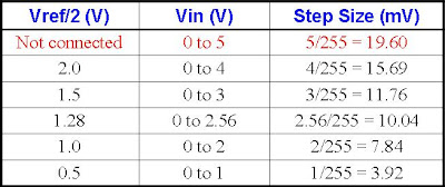
Where the Vcc is the reference voltage of ADC with n-bit resolution.Below is table in which Resolution versus Step Size for ADC (if Vcc = 5V) is provided.
Resolution versus Step Size for ADC
ADC0804 Chip (Free Running Mode)
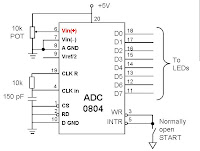
There are some control PINs and some input and other are output PINS of ADC0804. The pin configuration of ADC0804 is shown in the figure below.
ADC0804 Chip Free Running Mode
Important pins are discussed here in some detail.
CS  :Active low input used to activate the ADC0804 chip.

RD (data enable)  : Active low input used to get converted data out of the ADC0804 chip. When CS = 0, if a high-to-low pulse is applied to the RD pin, the 8-bit digital output shows up at the D0-D7 data pins.

WR (start conversion): Active low input used to inform the ADC0804 to start the conversion process. If CS = 0 when WR makes a low-to-high transition, the ADC0804 starts converting the analog input value of Vin to an 8-bit digital number. When the data conversion is complete, the INTR pin is forced low by the ADC0804.
CLK IN and CLK R : Connect to external capacitor and resistor for self-clocking, f = 1/(1.1RC). The clock affect the conversion time and this time cannot be faster than 110 micros.

INTR (end of conversion) This is an active low output pin. When the conversion is finished, it goes low to signal the CPU that the converted data is ready to be picked up. After INTR goes low, we make CS = 0 and send a high-to-low pulse to the RD pin to get the data out of the ADC0804 chip.
ADC0804 Chip step size calculation


Vin (+) and Vin (-) :These are the differential analog inputs where Vin = Vin (+) - Vin (-). Often the Vin (-) pin is connected to ground and the Vin (+) pin is used as the analog input to be converted to digital.
VCC : This is the +5V power supply. It is also used as a reference voltage when the Vref/2 (pin 9) input is open.
ADC0804 Chip step size calculation ADC0804 has resolution of 8 bits
Pin Vref/2 is open, Step size =19.6mV

Vref/2 :- Input voltage pin used for the reference voltage. If this pin is open, the analog input voltage for the the ADC is ranged from 0 to 5 volts.This is optional input pin. It is used only when the input signal range is small. When pin 9 is at 2V, the range is 0-4V, i.e. Twice the voltage at pin 9. Pin 6 (V+), Pin 7(V-): The actual input is the difference in voltages applied to these pins. The analogue input can range from 0 to 5V.

D0 – D7 output PINs of ADC: D0 – D7 are the digital data output pins. These are the tri-state buffered and the converted data is accessed only when CS = 0 and RD is forced low. The output voltage:


Analog Ground and Digital Ground :- Analog ground is connected to the ground of the analog signal while digital ground is connected to the ground of the Vcc pin.
Operation of the ADC
The analog signal should be connected to Vin.
To start conversion: WR should be pulled low and RD should be high.
When the conversion is complete, the ADC0804 will pull INT low.
To make the binary result available at the outputs of the ADC, RD should be low.

Tags:-
Digital Audio Compression Storage and Retrieval System (DACSRS),‑The ADC0804 is a successive approximation type A/D converter ,connection of temperature sensor with ADC0804 ,Automated Object Avoiding Robot Project,Transducer coverts physical variable to an electrical signal ,Design and implementation of frequency converter and signal recovery circuits. ,ADC0804 IC is a CMOS 8-bit A/D converter featuring fast conversion times,DATA CONVERSION,LEVEL & TEMPERATURE CONTROLLER, How to build a digital oscilloscope based on the ADC0804 Flashy acquisition board The interfacing of LM35 Temperature Sensor using ADC0804
read more "Schematic Analog-to-digital converter (ADC ) Interfacing with microcontroller"

Thursday, June 7, 2012

Schematic Microcontroller Applications and Analogue Interfacing for input and output

Microcontroller Applications and Analogue Interfacing for input and output

In this post we will learn how to Interface 8051 with the Input and Output Devices like Transducer/Sensors ,Analogue-to-Digital Conversion (ADC) and Digital-to-Analogue Conversion (DAC).These three types of Interfaces will be discussed in this post and some coming posts.

1. The interface of Transducer or sensors with Microcontroller 8051:-

The 8051 microcontroller is a general purpose microcontroller and widely used for different types of applications including industrial applications. In the process or even anyindustry there are many process parameters which are desired to be measured and process by microcontrollers for some suitable decisions. These process variables are sensed or measured by using appropriate sensors or transducer.As the digital computer and microcontrollers use binary values but in the physical world most things (like process variables in industry i.e temperature, pressure, humidity, etc) is in analog nature (continuous).
Thus the data to be measured of these parameters namely for example temperature, pressure, humidity, velocity, voltage are analog data. Most of the physical parameters are not in the form of electrical signals.A device called transducer is used to convert the physical quantity to electrical signals (i.e. voltage, current). One notable things is that the transducer are also referred to as sensors.
Sensors for temperature, velocity, pressure, light, and many other natural quantities can produce an output voltage (or current) which the value is proportional to the quantity being measured.
Then an analog-to-digital converter is used to translate the analog voltage to digital numbers so that microcontroller can read and process them. Lets take only the temperature for better understanding.

Temperature sensors :-

There are a wide variety of temperature sensors on the market today, including Thermocouples, Resistance Temperature Detectors (RTDs), Thermistors, Infrared, and Semiconductor Sensors.Most electronic temperature sensors used in engineering fall into one of two classes: resistive or thermoelectric. But this is not a boundary line as well i think.A more general classification of temperature sensors thermocouples, resistive sensors, bi-metallic sensors, infrared sensors, pyrometry based sensors, semiconductor sensors and thermographic liquid crystals.

Resistance Temperature Detector (RTD)

The RTD is a temperature sensing device whose resistance changes with temperature. Typically built from platinum, though devices made from nickel or copper are not uncommon, RTDs can take many different shapes.To measure the resistance across an RTD, apply a constant current, measure the resulting voltage, and determine the RTD resistance. We then use a resistance vs. temperature plot to determine the temperature of the surrounding medium.). RTDs exhibit fairly linear resistance to temperature curves over their operating regions, and any non-linearities are highly predictable and repeatable.

Thermistor

Thermistors are semiconductor based transducers, manufactured in the shape of flat disc, beads, or rods. They are manufactured by combining two or more metal oxides. Similar to the RTD, the thermistor is a temperature sensing device whose resistance changes with temperature. Thermistors, however, are made from semiconductor materials.). Resistance is determined in the same manner as the RTD, but thermistors exhibit a highly nonlinear resistance vs. temperature curve.Like the RTD, thermistors require external current excitation and significant signal conditioning. Chips do exist that will convert a thermistor value directly to digital data (MAX6682, Maxim / Dallas Semiconductor.

IC Temperature Sensors

RTDs and thermistors may be simple devices, but they are likely not suited to any mechatronics application. We need to buy the sensor, purchase a chip or create our own circuitry to apply a constant current and measure the resulting voltage, and run this output through and ADC. All these components need to be matched, for example the ADC needs to have high enough resolution to take advantage of the 5mv/°C change from the ADT70. This can end up being quite complicated and costly.

Thermocouples

When two dissimilar metals are in contact with each other, a thermal load existing over the junction of the metallic couple induces a measurable electrical potential. A thermocouple is a self-generating transducer made up of two or more junctions between dissimilar metals. It will be noted that one junction (the cold junction) has to be maintained at a known reference temperature, for instance by surrounding it with melting ice. The other junction is attached to the object to be measured. . The junctions between the two wires and the voltmeter do not cause any error signal to appear as long as they are at the same temperature. Since there is no proper reference junction with this approach, the system is liable to give an erroneous output if the temperature of the surrounding environment changes. This small error may be avoided by using a cold junction compensation system in which the characteristics of the signal conditioning circuitry are modified by including another temperature sensor such as a thermistor in the circuitry.

Semiconductor diode temperature sensors

PN junctions in silicon have become popular as temperature sensors due to their very low cost.The forward bias characteristic of a silicon diode is used here for temperature sensing. It is well-known that a voltage Vf has to be applied across the junction before a current will flow. For silicon Vf (which is often termed the diode voltage drop) is of the order of 600-700 mV. Vf is temperature dependent, and is very nearly linear over the temperature range from – 50 to + 150 °C. The voltage Vf has a temperature characteristic which is essentially the same for all silicon devices of about - 2 mV/°C.

Liquid crystal temperature sensors

A number of liquids (mainly organic) than be made to exhibit an orderly structure, in which most or a1l of the molecules are aligned in a common direction. The structure can be altered by electric or magnetic fields. Most people are familiar with the liquid crystal displays used in watches and calculators which use compounds sensitive to electric fiends. Less well- known, however, is the fact that some liquid crystal materials are temperature sensitive.

Temperature sensors (LM34 and LM35)

LM34 series are precision integrated-circuit temperature sensors whose output voltage is linearly proportional to Fahrenheit temperature. LM35 series are precision integrated-circuit temperature sensors whose output voltage is linearly proportional to Celsius temperature. They require no external calibration since it is internally calibrated. Their output voltage changes 10mV for each degree of temperature change.
Item        Temperature Range             Accuracy          Output
LM34      -50 F to +300 F                 +3.0 F             10 mV/F
LM34C    -40 F to +230 F                +3.0 F             10 mV/F
LM35      -55 °C to +150 °C             +1.5 °C           10 mV/°C
LM35C    -40 °C to +110 °C            +1.5 °C           10 mV/°C
LM35D     0°C to +100°C                +2.0°C            10 mV/°C
The LM34 an LM35 series are precision integrated-circuit temperature sensors.

Tags:-Microcontroller Applications,Thermistor,Temperature and Heat Transfer Measurements ,About Temperature & Moisture Sensors Devices & Uses in Measurement,proximity sensor interfacing with microcontroller ,Analog Temperature Sensors ,types of temperature sensors,pressure sensors,temperature sensors wiki,infrared temperature sensors,Direct Sensor-to-Micro controller Interface Circuits,temperature sensors pdf,thermocouple,temperature measurement,Universal Transducer Interface,temperature sensor circuit diagram,infrared heat sensors,flux heat,temperature sensor,5v precision voltage reference temperature transducer,Microcontroller to Sensor Interfacing Techniques, Design and Development of Microcontroller Based Auto-Flow Assembly ,temperature transducer suppliers,DNA TECHNOLOGY - Interfacing ADC0808 To 8051,pt100 sensor interface WITH ADC ,temperature transducer manufacturers,thermistor temperature circuit,Measuring The Output Signal of The Universal Transducer Interface ,thermistor transducer,matron dst100,The MCR temperature measuring transducers are available for resistance thermometers and thermocouples.interfacing of a sensor with the micro controller,metal sensor interfacing with micro controller
read more "Schematic Microcontroller Applications and Analogue Interfacing for input and output"

Monday, June 4, 2012

Schematic Programming Aspects of Moving message display project using 8051

Programming Aspects of Moving message display project using 8051:-
In this post we will discuss the software or program or code written for moving message display project using microcontroller 8051.
In this section, we will try to answer the issues related to the timings of the signals generated. The timing of the signal relates to the order in which an instruction or command is sent to the LCD along with the appropriate signal of control signals. For example, if the Microcontroller programmer intends to send a byte of data intended for the display screen; the programmer will follow the following pseudo code steps:
 Clear R/S signal to indicate an instruction is being sent
 Clear R/W signal to indicate writing to the LCD is being intended
 Move data to the data lines
 Set Bit EN signal and then Clear EN to indicate that data intended to the LCD is present on the connecting interface latch
 Check for Busy Flag to be set to logic zero. This to ensure that when next time data is to be sent to the LCD module, the LCD is not in the middle of performing any internal operations [4].
5.1 Code Overview
In this section, we will discuss some of the important sections of the code written for the Microcontroller. The code for the convenience of the reader is produced here as well as present in the soft copy in the attached files.
BUFFER EQU 05FH ;LOCATION FOR STORAGE LCD DATA
BUFF_POINTER EQU 05EH ;LOCATION HOLDS BUFFER CURRENT POINTER
DATA_LINE EQU 090H ;WRITING TO PORT 1
ORG 0000H
LJMP MAIN
;********************SERIAL ISR**********************************
ORG 0023H
PUSH ACC
PUSH 00H
LCALL SERIAL_ISR
POP 00H
POP ACC
RETI
;****************************************************************
;LCD CONTROL SIGNALS
LCD_EN EQU 0B7H
LCD_RW EQU 0B6H
LCD_RS EQU 0B5H
;LCD CONFIGURATIONS COMMANDS
FNC_SET EQU 38H ;8 BIT ,2 LINE , 5X7 MATRIX
ENT_MOD EQU 06H
;DIFFERENT SETTINGS OF BLINK,DISPLAY AND CURSOR ON/OFF
DOF_COF_BOF EQU 08H
DOF_COF_BON EQU 09H
DOF_CON_BOF EQU 0AH
DOF_CON_BON EQU 0BH
DON_COF_BOF EQU 0CH
DON_COF_BON EQU 0DH
DON_CON_BOF EQU 0EH
DON_CON_BON EQU 0FH
CLR_DISP EQU 01H
HOME_CUR EQU 02H
;DIFFERENT SETTING OF CURSOR/DISPLAY SHIFT RIGHT/LEFT
CUR_L EQU 10H
CUR_R EQU 14H
DISP_L EQU 18H
DISP_R EQU 1CH
;**************************************************************
MAIN:
MOV R0,#BUFF_POINTER
MOV @R0,#BUFFER ;STORE THE INTIAL POINT OF WRITING STRING
;START TIMER 1 FOR BAUD RATE GENERATION
MOV TMOD,#21H
MOV TH1,#-26
MOV TL1,#-26
SETB TR1
MOV SCON,#50H ;INIT THE SERIAL PORT FOR RECEPTION
MOV IE,#90H ;ENABLE SERIAL INTERUPT
MOV P1,#0H
MOV P3,#0H
MOV R0,#BUFFER+1
MOV @R0,#'A'
INC R0
MOV @R0,#'B'
INC R0
MOV @R0,#'C'
INC R0
MOV @R0,#0H
MOV R7,#1H ;100 ;SET DELAY TIMER
;LCALL DELAY
;LCALL INIT
LCALL PRINT_STR
SJMP $
;*************************** DELAY ROUTINE *************************
;THE ROUTINE PRODUCES A DELAY OF 10 msec
;VALUE EXPECTED IN R7, FOR NUMBER OF TIMES
;TO RUN THIS FUNCTION
DELAY:
AGAIN:
MOV TH0,#HIGH(-10000)
MOV TL0,#LOW(-10000)
SETB TR0
JNB TF0,$
CLR TF0
CLR TR0
DJNZ R7,AGAIN
RET
;********************************************************************
;******************INITIALIZATION AND RESEST ROUTINE FOR LCD********
INIT:
CLR LCD_EN
CLR LCD_RW
CLR LCD_RS
MOV R7,#FNC_SET ;WRITING FUNCTION SET TO LCD
LCALL WRITE_LCD_INST
MOV R7,#01H ;GIVE 10MS DELAY
MOV R7,#FNC_SET ;WRITING FUNCTION SET TO LCD
LCALL WRITE_LCD_INST
MOV R7,#01H ;GIVE 10MS DELAY
MOV R7,#FNC_SET ;WRITING FUNCTION SET TO LCD
LCALL WRITE_LCD_INST
MOV R7,#01H ;GIVE 10MS DELAY
MOV R7,#DOF_COF_BOF
LCALL WRITE_LCD_INST
MOV R7,#DON_CON_BOF
LCALL WRITE_LCD_INST
MOV R7,#CLR_DISP
LCALL WRITE_LCD_INST
MOV R7,#ENT_MOD
LCALL WRITE_LCD_INST
RET
;*********************************************************************
;*********************WRITING COMMANDS TO LCD*************************
;THE COMMAND TO BE SENT IS PLACED IN R7
WRITE_LCD_INST:
CLR LCD_EN
CLR LCD_RS
CLR LCD_RW
MOV DATA_LINE,R7
SETB LCD_EN
CLR LCD_EN
LCALL CHK_BZ_FLAG
MOV R7,#02H
RET
;*************************************************************
;****************************************************************
;******CHECKS FOR BUSY FLAG FOR THE LCD*******************
;READS LCD STATUS AND CHECKS BZ FLAG IN MSB OF DATA_LINE
CHK_BZ_FLAG:
CLR LCD_EN
SETB LCD_EN
CLR LCD_EN
MOV DATA_LINE,#0FFH ;TO CONFIGUREPORT TO READ INPUT
SETB LCD_RW
PUSH ACC
CHK_PULSE:
SETB LCD_EN
MOV A,DATA_LINE
CLR LCD_EN
JB ACC.7,CHK_PULSE
POP ACC
CLR LCD_RW
RET
;**************************************************************************
;************************WRITING DATA TO LCD*******************************
;WRITES DATA TO LCD. ACCEPTS DATATO BE SENT IN R7
WRITE_LCD_DATA:
CLR LCD_EN
SETB LCD_RS
CLR LCD_RW
MOV DATA_LINE,R7
SETB LCD_EN
CLR LCD_EN
CLR LCD_RS
LCALL CHK_BZ_FLAG
RET
;**************************************************************************
;*********************PRINTS THE CONTENTS OF BUFFER************************
;bUFFER LOCATION HOLDS THE STRING TO BE TRANSMITTED,IT IS 0 TERMINATED
PRINT_STR:
MOV R0,#BUFFER+1
PRINT_NEXT:
CJNE @R0,#30H,PRINT
SJMP END_STR
PRINT:
MOV A,@R0
MOV R7,A
LCALL WRITE_LCD_DATA
INC R0
SJMP PRINT_NEXT
END_STR:
RET
;************************************************************************
;*************************SERIAL ISR HANDLER*****************************
SERIAL_ISR:
CLR RI
MOV A,SBUF
CJNE A,#30H,STORE_VALUE
MOV R0,BUFF_POINTER
MOV @R0,#0H
LCALL PRINT_STR ;PRINTS THE RECIVED STRING
RET
STORE_VALUE:
MOV R0,BUFF_POINTER
MOV @R0,A
INC R0
MOV BUFF_POINTER,R0
RET
END
Tags:-
Programming Aspects of Moving message display project using 8051,assembly language program for lcd,software named Proteus 7 for simulating the working of our project,8051software ,8051 Software, C Compilers, Basic Editor, and Chip Simulator, PC-based programs, and a development board ,develop your 8051-based project, 8051 Software Tools Overview,Free 8051 Tools, Code and Projects,Free 8051 microcontroller resources,Easy To Use Monitor Program, AS31 Assembler, Development Circuit Board Design, Code Library ,Code Library ,8051 Code Examples,Assembly Language Programming: 8051,Test code for 8051SBC ,An introduction to the 8051, especially programming the 8051 in C using the Keil ,8051 code, with serial port code, math functions,program ming Phillips not working with Atmel code 8051‎ ,Assembly code for 1sec delay for 8051‎ ,How to write the 8051 program to control the alarm,Programming and Interfacing the 8051 in C and Assembly,8051 program code to HD44780 ,8051 microcontroller hardware interfacing tutorials ,8051 Microprocessor Example Program,ACCESSING CODE ROM SPACE IN 8051 C,Free 8051 Microcontroller projects
read more "Schematic Programming Aspects of Moving message display project using 8051"

Schematic Hardware Aspects of Moving Message Display Project

Hardware Aspects of Moving Message Display Project:-
The moving message display is fabricated using these major components:-
1. Micro controller AT89s51
2. LCD
3. RS-232
4. Computer
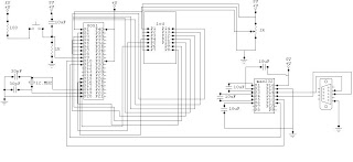
the moving message will be display on the LCD which will be controlled through microcontroller and the message will be sent by computer using RS232. The circuit diagram of the moving message display is shown in this post and how the whole process is completed is discussed here.
The Microcontroller in this software is programmed such that it controls the LCD through an interface. An eight-bit interface between in the LCD and Microcontroller is programmed to transfer the data to be written on the LCD display screen. A further three out pins of the Microcontroller are used to generate control signals for the LCD. The three control signals are generated in the same pattern as discussed in the timing diagram in the previous chapters.
The project, when looked in totality, can be seen as composing of three components, namely LCD, Microcontroller and serial port. The three components have been discussed independently until now and to give a complete picture, it is necessary to link these components. The linking is not only logical but is also translated into hardware connections.
4.1 Serial Port to Microcontroller
The serial port is connected to the Microcontroller to provide the end user with the functionality of passing a desired string to LCD in run time. An interface between the serial port and the Microcontroller is required for the data transfer.
A variable baud rate is generated by the Microcontroller to synchronize the data transfer between the two ends. The connectivity can be analyzed and understood by the hardware diagram at the end of the chapter.
4.2 Microcontroller to LCD
The Microcontroller connects with the LCD with an 8bit interface to for data transfer. Three further pins are required to generate enable, read/write and instruction / data signals for the LCD. These three form a small instruction set that allows different tasks and the functionality provided by the HD44 LCD.
4.2.1 Enable Signal Connection
The enable signal is used as a signal to the LCD by the Microcontroller about the availability of data. A high-to-low edge triggers the LCD into reading its data lines. The data meant for the LCD must be present and latched on the data lines before the enable signal switches from high to logic low. It needs to be understood that data lines for sending instructions and display data are the same, the instruction bits help differentiate among the two for the LCD.
4.2.2 Read/Write Signal Connection
The read/write signal specifies to the LCD whether the Microcontroller is intends to read data from its DDRAM/CGRAM or intends to write data to its DDRAM/CGRAM. In the former case, the data lines contain the data meant for the destination on the LCD memory and in the latter case; the data lines will have the data written onto from the appropriate DDRAM/CGRAM.
4.2.3 Instruction/Data Signal Connection
The instruction/data line specifies whether the data bus contains an instruction or data meant for the LCD. This signal, along with the instruction bits, help LCD in deciding which control signals to generate to fulfill the request.
Hardware Aspects of Moving Message Display Project, circuit diagram of movinging message display using microcontroller 8051


4.2.4 Busy Flag
After sending of every request, whether instruction or data, to the LCD; the Microcontroller must check for the busy flag of the LCD to return to low logic again. A high logic for the busy flag signals that an internal operation is being carried out and during this time, no external instruction or data is entertained. Only when the busy flag is at a logic low, the Microcontroller should send the next instruction or data. The busy flag is checked by configuring the LCD into read mode (R/W signal is set to logic high) and then reading the data lines. The MSB of the byte read contains the value of the busy flag. To understand the above concepts, the timing diagram mentioned in Chapter 2 for busy flag testing and data transfer may be used.


Tags:-
Hardware Aspects of Moving Message Display Project,LED BASED MOVING DISPLAY USING 8051 ,Scrolling Message in LED Display with 8051,8x8 LED Matrix using 8051‎ ,A Microcontroller Based Moving Message Display,Project Help / Display Moving Message ,scrolling message display using 8051,LCD and computer PC,Microcontroller Based moving message display,8051 based Moving massage display‎ ,8051 message display, microcontroller moving message display, circuit for moving message display, This is the report of the mini project we did in our sixth semester of Engineering. It uses a at89c51 microcontroller to display 16 messages in moving,moving message display using Lcd and 8051 microcode ,build a moving message display board with 8051 microcontroller,
read more "Schematic Hardware Aspects of Moving Message Display Project"

Schematic Introduction to 89C51 Microcontroller

Introduction to 89C51 Microcontroller:
The ATMEL 89C51 is used here; some of the features with respect to our project are discussed here.
3.1 Memory Organization
The ATMEL 89C51 implements a separate memory space for code and data, both code and data may be internal; however, both expand using external components to a maximum of 64k code memory and 64k data memory. The memory consists of on-chip ROM (4KB) and on-chip RAM (128B). The on-chip RAM contains rich arrangements of general-purpose storage, bit addressable storage, register banks, and special function registers (SFR’s). The notable features are
• The registers and input/output ports are memory mapped
• The stack memory resides within the internal RAM
3.1.1 General-Purpose RAM
There are total of 80 bytes of general-purpose RAM from address 30H to 7FH. Any location in this part can be addressed using direct or indirect addressing modes.
3.1.2 Bit-Addressable RAM
The ATMEL 89C51 contain 210 bit-addressable locations, of which 128 are at byte addresses 20H through 2F, and the rest are in SFR’s. Bits can be set, cleared, ANDed, ORed, etc with a single instruction. These bits can be accessed as bytes or as bits.
3.1.3 Register Banks
The bottom 32 locations of internal memory contain the register banks, each having registers from R0 to R7. The different banks are selected using register bank select bits (RS0 and RS1) in program status word.
3.1.4 Special Function Registers
The ATMEL 89C51 internal registers are configured as a part of on chip RAM: therefore each register also has an address. There are 21 special function registers, each having a name and direct address, for example accumulator has name A and address ACC.
3.2 Input/output Ports
3.2.1 Port 0
Port 0 is a dual-purpose serving as general-purpose I/O port. For larger design it is used to multiplex the low byte of 16-bit address.
3.2.2 Port 1
Port 1 is a dedicated I/O port, used for interfacing to external devices. No alternate functionality is defined for the port.
3.2.3 Port 2
Port 2 is a dual-purpose port serving as general –purpose I/O port, or as high byte of address bus for designs with external code memory exceeding 256 bytes.
3.2.4 Port 3
Port 3 is a dual-purpose port serving also as general-purpose I/O port, the individual pins of the port 3 also has some special features.
3.3 Interrupts
There are total of five interrupts in ATMEL 89C51 as given below
• Two for external interrupts INT0 and INT1
• Two for timer1 and timer0
• One for serial port
3.4 Two 16-bit Timers
The ATMEL 89C51 have two 16-bit timers, controlled by TCON register. They can be operated in four different modes named: 13-bit timer mode, 16-bit timer mode, 8-bit auto-reload mode, and split-timer mode. The mode and clocking sources of timer0 and timer1 are set by TMOD register. Other registers that are used in timer operation are THx, and TLx. The timer is started by setting the flag TRx and when an overflow occurs the TFx flag is set automatically.
3.5 Serial Interface
The ATMEL 89C51 serial port has four modes of operation, named 8-bit shift register mode (fixed baud rate), 8-bit UART mode (variable baud rate), 9-bit UART mode (fixed baud rate), and 9-bit UART mode (variable baud rate). The timer1 is used for setting the variable baud rate. The different flags used in serial interfacing are TI and RI.
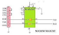
3.5.1 MAX 232 Serial Interface IC
MAX 232 Circuit Diagram MAX 232 converts serial data into parallel in receiving mode Introduction to 89C51 Microcontroller


MAX 232 converts serial data into parallel in receiving mode while it converts parallel data into serial in transmitting mode. Standard serial interfacing for PC, MAX232, requires negative logic, i.e., logic '1' is -5V to -12V and logic '0' is +5V to +12V. To convert TTL logic, say, TxD and RxD pins of the microcontroller chips thus need a converter chip. A MAX232 chip has long been using in many microcontroller boards. It provides 2-channel RS232C port and requires external 10uF capacitors. Carefully check the polarity of capacitor when soldering the board.


Tags:-MAX232 Serial level converter ,Serial Programming/MAX232 Driver Receiver ,Interfacing The Serial / RS-232 Port,pin diagram of atmel 89C51 atmel 89C51 pin diagram 8051 Tutorial: Interrupts 8051 Microcontroller Architecture The 8051 Microcontroller and Embedded Systems INTERRUPTS PROGRAMMING IN ASSEMBLY Define the interrupt priority of the 8051 MEMORY AND REGISTER ORGANISATION 8051 Memory Organisation. Internal ROM. The 8051 has 4K (4096 locations) of on-chip ROM. This is used for storing the system program. 8051 MEMORY ORGANIZATION, PROGRAM MEMORY, DATA MEMORY 8051 Memory Write Example Program
read more "Schematic Introduction to 89C51 Microcontroller"